
Surface plasmon devices

a surface plasmon and plasmon technology, applied in the direction of instruments, semiconductor lasers, optical elements, etc., can solve the problems of inability to operate at terahertz frequencies or higher, limited device speed, and relatively expensive fabrication of semiconductor-based devices,

Inactive Publication Date: 2006-03-07
UNIV OF COLORADO THE REGENTS OF
View PDF7 Cites 165 Cited by
  • Summary
  • Abstract
  • Description
  • Claims
  • Application Information

AI Technical Summary

Benefits of technology

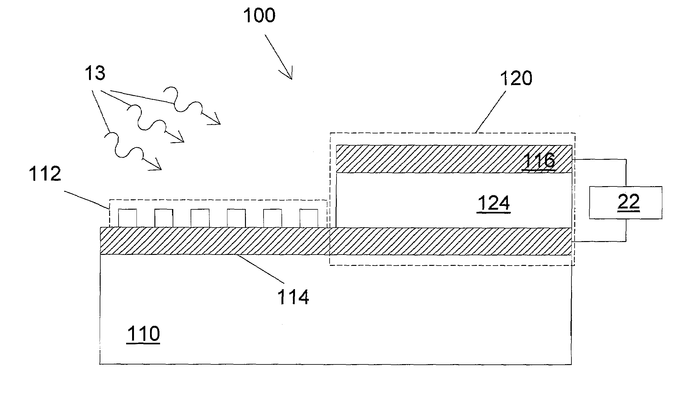
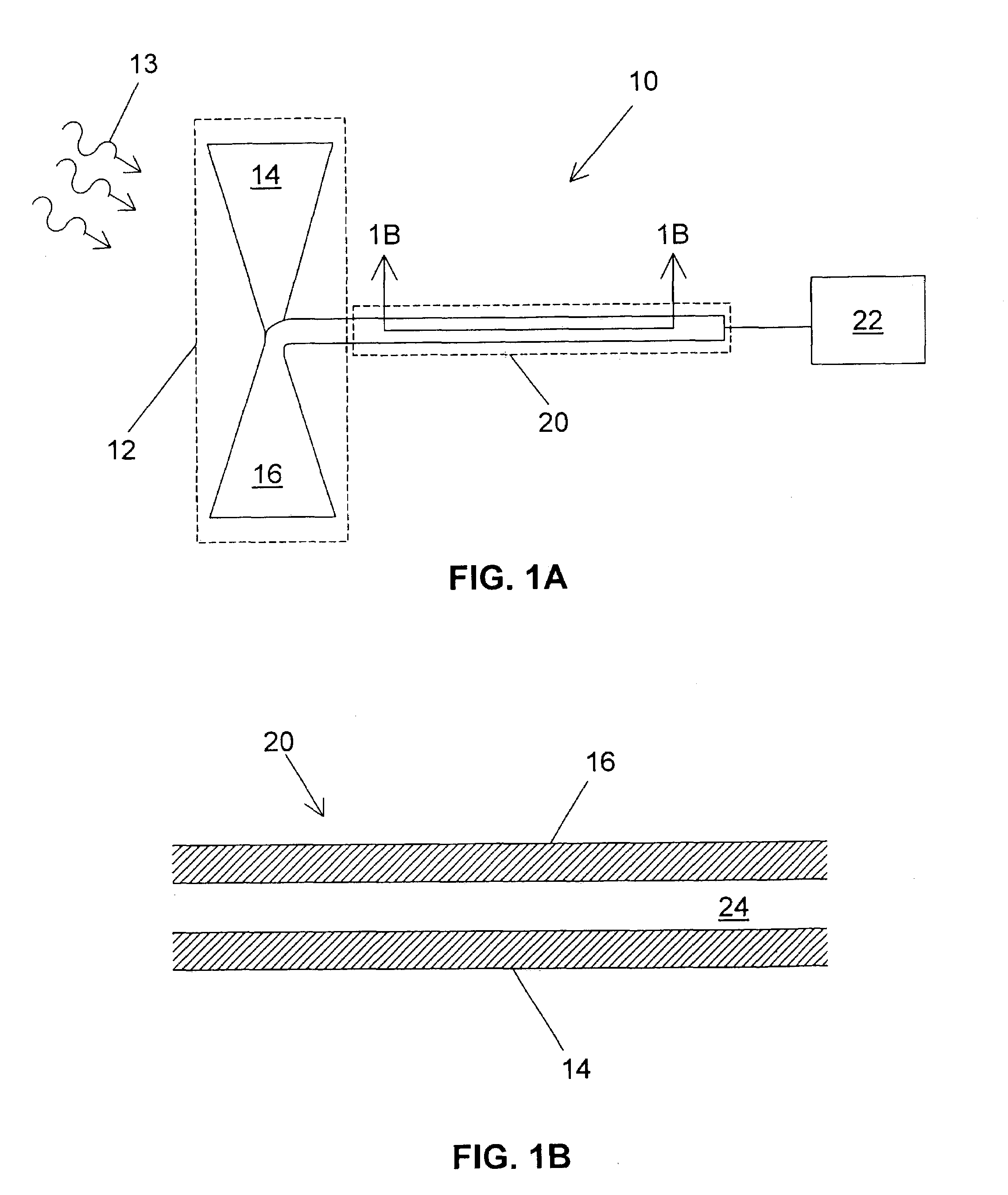
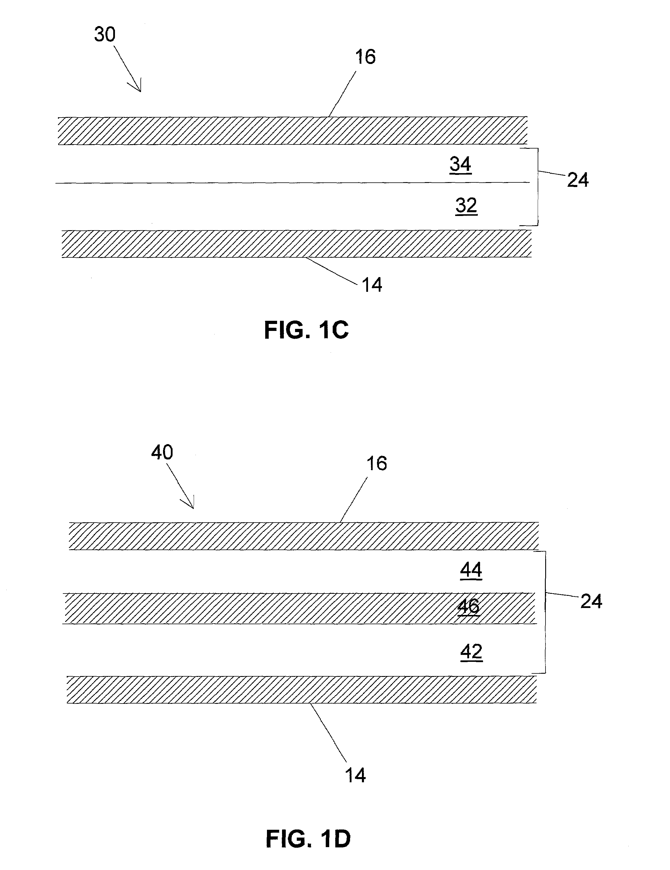
[0040]As will be described in more detail hereinafter, there is disclosed herein a device designed in accordance with one aspect of the present invention and including an input port, which input port is configured to receive an input signal, and an output port. The device also includes a structure, which structure in turn includes a tunneling junction connected with the input port and the output port. The tunneling junction is configured in a way (i) which provides electrons in a particular energy state within the structure, (ii) which produces surface plasmons in response to the input signal, (iii) which causes the structure to act as a waveguide for directing at least a portion of the surface plasmons along a predetermined path toward the output port such that the surface plasmons so directed interact with the electrons in a particular way, and (iv) which produces at the output port an output signal resulting from the particular interaction between the electrons and the surface plasmons.

Problems solved by technology

One of the disadvantages of conventional electronic devices based on electron charge oscillation is that they cannot operate at terahertz frequencies or higher due to time constant limitations.
In tunneling junction devices, for example, the speed of the device is limited by the fact that the outer conductive layers of the tunneling junctions act as parallel plate capacitors.
Due to their crystalline nature and the fact that deposited semiconductor layers must epitaxial, semiconductor-based devices are relatively expensive to fabricate and very difficult to integrate with other optoelectronic devices.
One consequence of the lower carrier concentration is that the plasma frequency is reduced from optical frequencies to millimeter wave frequencies, so that optical waves cannot be carried by semiconductor surface plasmons.
Still another consequence for amplification and emission devices is that the increased resistance would limit the output intensity and increase heating.
One such drawback is the relatively inefficient spontaneous emission process of surface plasmons in single-insulator MIM diodes.
For example, Volkov and Chuiko estimate the efficiency of this transition to be ˜10−4.7 To improve the spontaneous emission efficiency, Aleksanyan et al. investigated insulator structures with one or more quantum wells in which the quantized energy levels inside the potential wells limit the available tunneling states to those for inelastic tunneling in which a surface plasmon is generated.8 A problem with embodiments in the literature devices based on multiple quantum well structures is the non-uniformity of the barrier and quantum well layers.
It is submitted that traditional thin film deposition techniques, such as evaporation, are not well suited for growing very thin (<5 nm) uniform layers of amorphous materials due to the difficulty in controlling the uniformity of layers.
Another drawback of the Lambe device is the inefficient output coupling of surface plasmon waves to optical radiation.
This approach has the disadvantages that the optical power must traverse the thickness of the top metal layer before radiating into free space, which is a lossy process.
Furthermore, for some applications, surface roughening is a rather uncontrolled method to couple out the light as the light will tend to radiate equally into the hemisphere above the device.
However, Siu et al. do not suggest practical applications for the phenomenon.
smons. Xie also considers stimulated emission and absorption of surface plasmons in MIM transition metal type like junctions.16 While Xie shows that stimulated emission of surface plasmons is theoretically possible in MIM devices, the material selection in the MIM diode as discussed in the article is very l
λ˜10 μm. Further, Xie restricts the outer metal layers of the MIM to single crysta
l metals. However, Xie does demonstrate the possibility of obtaining large gain from such devices and suggests that such a structure might be useful as an amplifier or emitter in the infrared region, although Xie does not discuss the possibility of gain in the visible or othe
Furthermore, none of the above references suggest methods for producing the necessary thin, uniform barrier and well layers for these devices.
This requirement adds cost to device fabrication and limits device integration with other optoelectronic devices.

Method used


Image

  • Surface plasmon devices
  • Surface plasmon devices
  • Surface plasmon devices

Examples


Embodiment Construction

[0087]The following description is presented to enable one of ordinary skill in the art to make and use the invention and is provided in the context of a patent application and its requirements. Various modifications to the described embodiments will be readily apparent to those skilled in the art and the generic principles herein may be applied to other embodiments. Thus, the present invention is not intended to be limited to the embodiment shown but is to be accorded the widest scope consistent with the principles and features described herein.

[0088]Although the aforedescribed prior art devices and theoretical disclosures regarding sophisticated manipulation of surface plasmons, such as stimulated emission and stimulated absorption, have been made over the past twenty-five years, the Applicants are unaware of presently available, practical devices that actually allow such manipulations. Recent progress in tunneling junction technology by the assignee of the present application has...


PUM

PropertyMeasurementUnit
optical frequenciesaaaaaaaaaa
temperatureaaaaaaaaaa
thickaaaaaaaaaa

Abstract

A device including an input port configured to receive an input signal is described. The device also includes an output port and a structure, which structure includes a tunneling junction connected with the input port and the output port. The tunneling junction is configured in a way (i) which provides electrons in a particular energy state within the structure, (ii) which produces surface plasmons in response to the input signal, (iii) which causes the structure to act as a waveguide for directing at least a portion of the surface plasmons along a predetermined path toward the output port such that the surface plasmons so directed interact with the electrons in a particular way, and (iv) which produces at the output port an output signal resulting from the particular interaction between the electrons and the surface plasmons.

Description

BACKGROUND OF THE INVENTION[0001]The present invention relates to surface plasmon devices and methods of making such devices and, more specifically, to surface plasmon guided wave devices whose optical frequency response is not limited by RC time constant.[0002]One of the disadvantages of conventional electronic devices based on electron charge oscillation is that they cannot operate at terahertz frequencies or higher due to time constant limitations. In tunneling junction devices, for example, the speed of the device is limited by the fact that the outer conductive layers of the tunneling junctions act as parallel plate capacitors. Coupled with the internal and external resistance to current flow, the RC time constant constrains the speed of the tunneling junction device. Thus, only very small devices, which have correspondingly small capacitance, can be operated at optical frequencies of 1013–1015 Hz.[0003]One way to circumvent the RC time constant limitation and get optical frequ...

Claims


Application Information

Patent Timeline
Patent Type & Authority Patents(United States)
IPC IPC(8): G02B6/12H01S3/04H04B10/06G02B6/122G02F1/017H01S5/10
CPCB82Y20/00G02B6/1226G02F1/017H01S5/1046G02F2203/10
Inventor ESTES, MICHAEL J.MODDEL, GARRETT
Owner UNIV OF COLORADO THE REGENTS OF
Learn More