Ceramic substrate for semiconductor production and inspection devices

a ceramic substrate and inspection device technology, applied in the field of ceramic substrates, can solve the problems of deterioration of temperature-rising properties or heat uniformity of ceramic substrates, and achieve the effects of improving heat uniformity, lowering heat conduction barriers, and improving sinterability

Inactive Publication Date: 2006-03-14
IBIDEN CO LTD
View PDF74 Cites 12 Cited by
  • Summary
  • Abstract
  • Description
  • Claims
  • Application Information

AI Technical Summary

Benefits of technology

[0008]The inventors of the present invention studied earnestly to solve the above problems. Consequently, they have found that the reason why the temperature-rising property or the heat uniformity of such a large ceramic substrate having a diameter exceeding 250 mm is deteriorated is the increase of a heat capacity of a ceramic substrate. Simultaneously, they have found that the temperature-rising property and the heat uniformity can be improved: by lowering a barrier of heat conduction between ceramic particles through the improvement of sinterability by incorporating oxygen in a ceramic substrate; and by the reduction of the heat capacity itself through the adjustment of the thickness of the ceramic substrate to 25 mm or less.
[0009]Moreover, in the case of a large ceramic substrate which has a diameter exceeding 250 mm, if the thickness thereof is adjusted to 25 mm or less, a warp tends to be generated at a high temperature. They have found that the warp can be prevented almost completely by: forming a conductor at the position of 60% in a thickness-direction from the bottom face opposite to a wafer treating face of the ceramic substrate; and using a nitride ceramic containing oxygen or an oxide ceramic as the ceramic. Thus, they have accomplished the present invention.
[0010]In case a disk-shaped ceramic substrate has a diameter of 250 mm or more, the ceramic substrate is adjusted to have a thickness of 25 mm or less in order to reduce the heat capacity of the ceramic substrate. In such a case, if a resistance heating element is disposed inside the ceramic substrate, the distance between the resistance heating element and the heating face becomes shorter correspondingly, resulting in an occurrence of a temperature distribution similar to the pattern of the resistance heating element. The present invention has been accomplished through the finding that disposing of a conductor, such as a resistance heating element, on the back side of a ceramic substrate makes it possible to keep the substantial distance between the heating face and the resistance heating element, and can improve the temperature-rising property and the heat uniformity.
[0011]Besides, although the adjustment of the thickness of a ceramic substrate to 25 mm or less makes the ceramic substrate apt to warp at a high temperature, the present invention can also prevent such a warp.

Problems solved by technology

There existed a problem that such enlargement of an electrostatic chuck and the like results in the deterioration of a temperature-rising property or a heat uniformity of a ceramic substrate, those are the properties being demanded at the production of semiconductor devices and the like.

Method used


Image

  • Ceramic substrate for semiconductor production and inspection devices
  • Ceramic substrate for semiconductor production and inspection devices
  • Ceramic substrate for semiconductor production and inspection devices

Examples


examples 1 to 3

Hot Plate (Reference to FIG. 9)

[0133](1) An aluminum nitride sintered body was obtained by: mixing 100 parts by weight of aluminum nitride powder (manufactured by Tokuyama Corp., average particle diameter 1.1 μm) which is fired in the air at 500° C. for one hour, 4 parts by weight of yttrium oxide (Y2O3: yttria, average particle diameter 0.4 μm) and 11.5 parts by weight of acrylic resin binder; putting the mixture into a hexagonal columnar mold; and then hot pressing it in a nitrogen atmosphere under the conditions: at a temperature of 1890° C. and a pressure of 150 kg / cm2 for three hours. Ceramic substrates having, respectively, a diameter of 280 mm and a thickness of 19 mm (Example 1), a diameter of 310 mm and a thickness of 5 mm (Example 2) and a diameter of 350 mm and a thickness of 3 mm (Example 3) were obtained by processing the above aluminum nitride sintered body into disk shapes and varying a surface grinding amount.

(2) A conductor containing paste was printed on the bottom...

examples 4 to 6

Alumina Hot Plate

[0140](1) Green sheets 50, which were 0.47 mm in thickness, were obtained: by using a paste containing alumina:93% by weight, SiO2:5% by weight, CaO:0.5% by weight, MgO:0.5% by weight, TiO2:0.5% by weight, an acrylic binder:11.5 parts by weight, a dispersant: 0.5 part by weight and 53 parts by weight of alcohol comprising 1-butanol and ethanol; and forming it by a doctor blade method.

(2) Subsequently, after drying these green sheets at 80° C. for 5 hours, to the green sheets having a necessity of being processed, portions which will become through holes, in which lifter pins for a semiconductor wafer, 1.8 mm, 3.0 mm and 5.0 mm in diameter, respectively, and portions which will become conductor-filled through holes for being connected with external terminals were formed by punching.

(3) Conductor containing paste B was prepared by mixing 100 parts by weight of tungsten particle having an average particle diameter of 3 μm, 1.9 parts by weight of an acrylic binder, 3.7 ...

examples 7 to 9

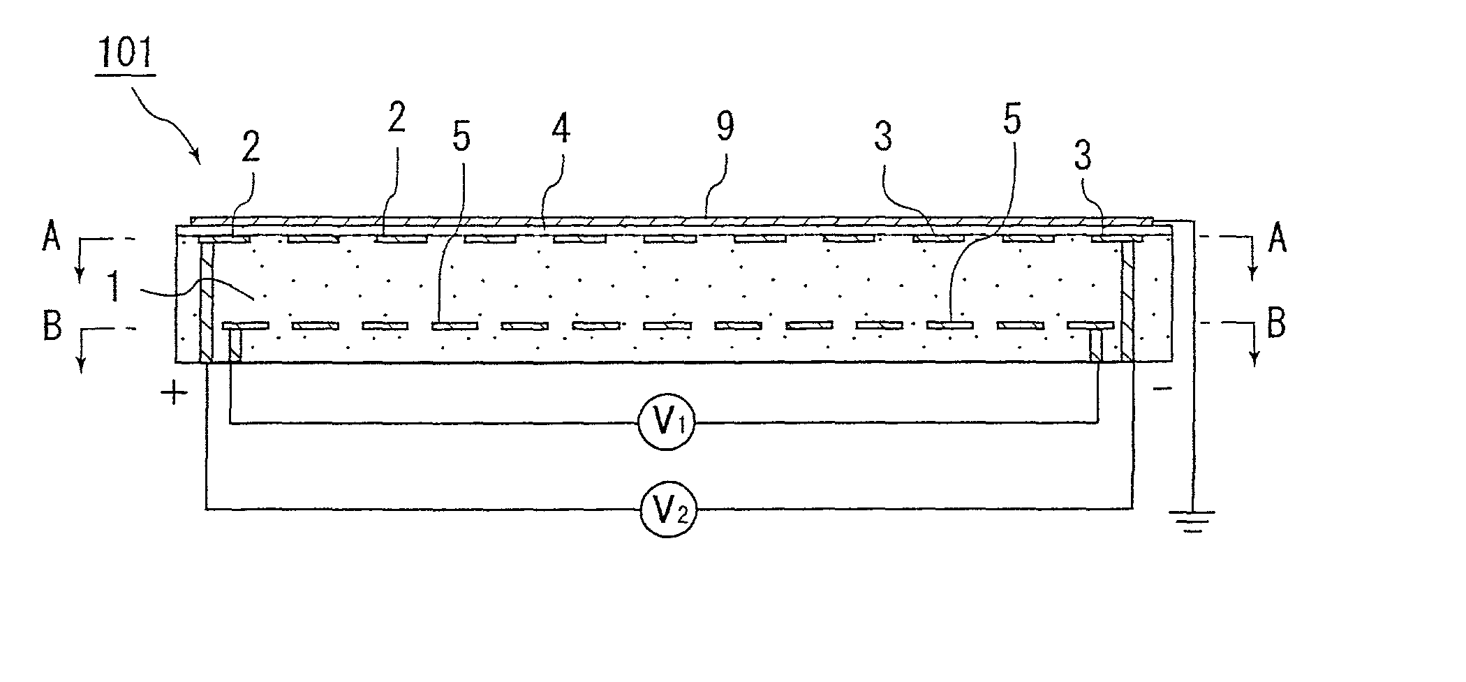
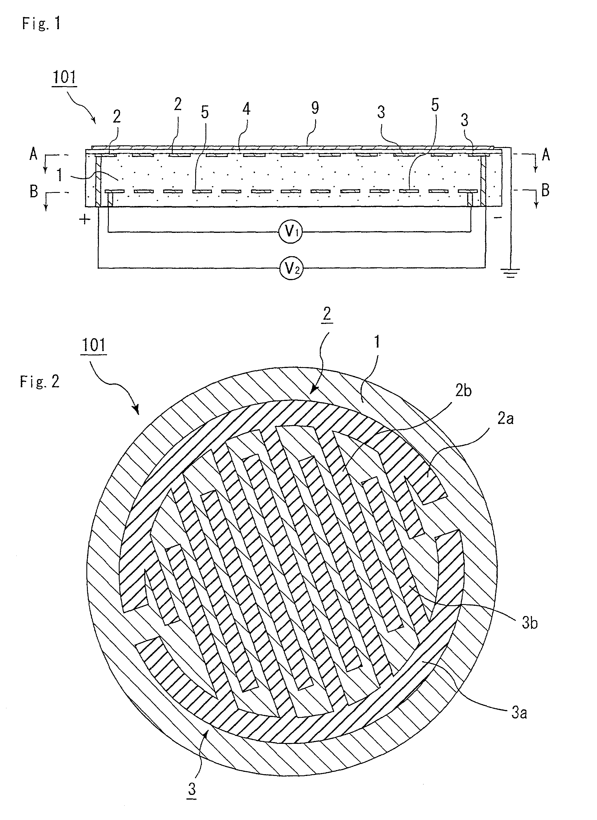
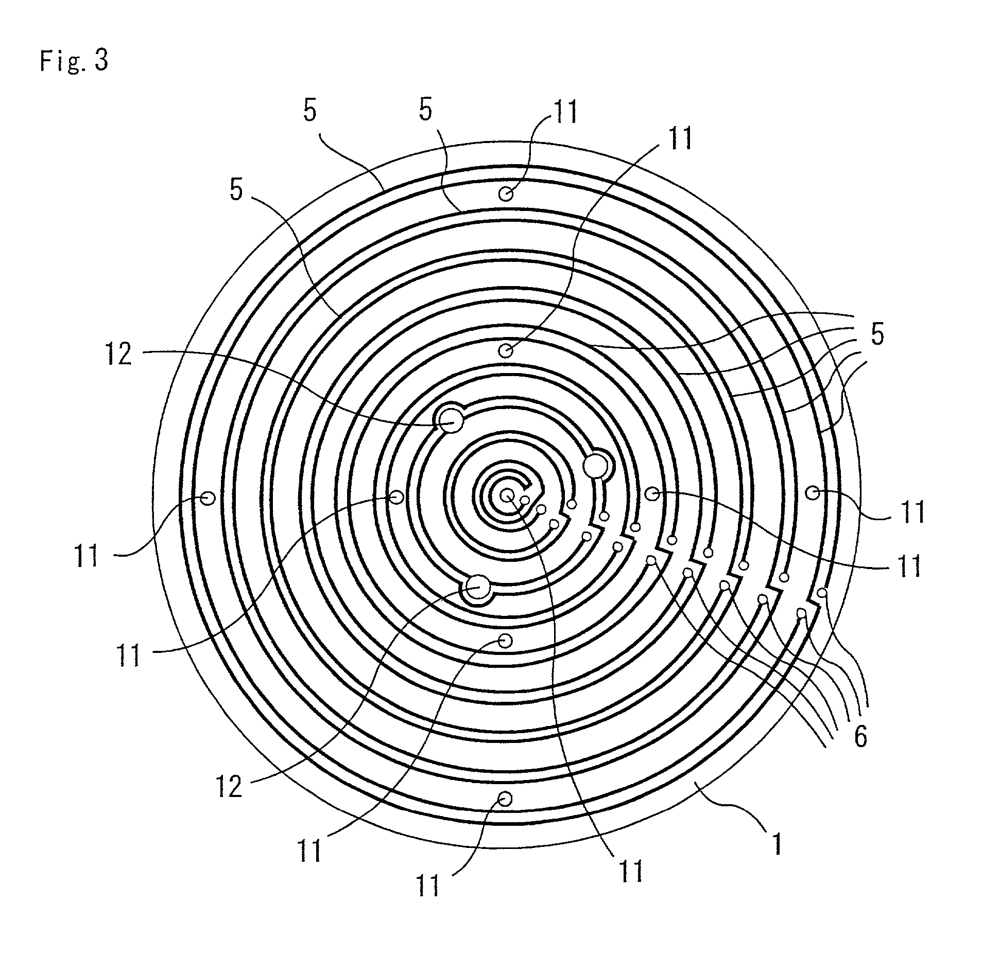
Manufacture of Electrostatic Chucks Made of AlN with Heaters (FIGS. 1 to 3)

[0149](1) Next, green sheets 50, which were 0.47 mm in thickness, were obtained by: using a paste prepared by mixing 100 parts by weight of aluminum nitride powder (manufactured by Tokuyama Corp., average particle diameter 1.1 μm) fired in the air at 500° C. for one hour, 1,2, 4 parts by weight of yttria (average particle diameter 0.4 μm), 11.5 parts by weight of acrylic binder, 0.5 part by weight of a dispersant and 53 parts by weight of alcohol comprising 1-butanol and ethanol; and forming it by a doctor blade method.

(2) Subsequently, after drying these green sheets 50 at 80° C. for 5 hours, to the green sheets having a necessity of being processed, portions which will become through holes, in which lifter pins for a semiconductor, 1.8 mm, 3.0 mm and 5.0 mm in diameter, respectively, and portions which will become conductor-filled through holes for being connected with external terminals were formed by punc...


PUM

PropertyMeasurementUnit
thicknessaaaaaaaaaa
thicknessaaaaaaaaaa
temperatureaaaaaaaaaa

Abstract

The object of the present invention is to provide a ceramic substrate that can provide a substantially uniform temperature distribution to a surface of the ceramic substrate where a semiconductor wafer is treated. A ceramic substrate for a semiconductor-producing/examining device according to the present invention is a ceramic substrate having a conductor formed on a surface of the ceramic substrate or inside the ceramic substrate, wherein said substrate is containing oxygen and having a disc form, the diameter thereof exceeding 250 mm and a thickness thereof being 25 mm or less.

Description

TECHNICAL FIELD[0001]The present invention relates mainly to ceramic substrates used as a device for producing or examining semiconductors, such as ceramic substrates for hot plates (ceramic heaters), electrostatic chucks and wafer probers.BACKGROUND ART[0002]As the device for producing or examining semiconductors including an etching device, a chemical vapor deposition device and the like, heaters or wafer probers and the like using substrates made of metal such as stainless steel or aluminum alloy, have been conventionally used.[0003]However, heaters made of metal have problems that they have poor temperature control characteristics and they are heavy and bulky since they are thick; and also have another problem that they have poor corrosion resistance to corrosive gases.[0004]In order to solve such problems, heaters which use ceramic such as aluminum nitride have been developed in place of heaters made of metal.[0005]Since such ceramic heaters have the advantage that a warp and t...

Claims


Application Information

Patent Timeline
Patent Type & Authority Patents(United States)
IPC IPC(8): B32B1/00H01L21/00H01L21/68H05B3/14H05B3/26H05B3/28
CPCH01L21/67103H01L21/6835H05B3/143H05B3/26H05B3/283H01L2924/19041Y10T428/21H05B2203/002H05B2203/014H05B2203/017H05B2203/032Y10T428/218
Inventor ITO, YASUTAKAHIRAMATSU, YASUJI
Owner IBIDEN CO LTD
Why Eureka
Try Eureka