High voltage transistor scaling tilt ion implant method

a technology of high-voltage transistors and tilt ion implants, which is applied in the direction of transistors, electrical apparatus, semiconductor devices, etc., can solve the problems of difficult to achieve optimized results within requisite tolerances, difficult to fabricate relatively small-sized high-voltage transistors with the ability to maintain requisite electrical relationships between component regions, and complicated semiconductor integrated circuit manufacturing efforts, etc., to facilitate fabrication, facilitate utilization of channel dopant halos, and minimal or no detrimental hot electron impacts

Inactive Publication Date: 2006-03-14
CYPRESS SEMICON CORP
View PDF7 Cites 32 Cited by
  • Summary
  • Abstract
  • Description
  • Claims
  • Application Information

AI Technical Summary

Benefits of technology

[0008]The present invention is a high voltage transistor formation method and system. A present invention high voltage transistor includes a varying or gradient concentration profile implant region. The implant region has a concentration profile that provides a higher concentration of dopants under the center of a source and drain region and a lower concentration close to the substrate surface and partially under a gate. This facilitates fabrication of smaller (e.g., with shorter channels) relatively high voltage signal switching transistors with minimal or no detrimental hot electron impacts. The gradient concentration qualities also facilitate utilization of channel dopant halos that provide increased breakdown resistance. A lightly doped drain tilt implant proc

Problems solved by technology

Fabricating relatively small sized high voltage transistors with the ability to maintain requisite electrical relationships between component regions is usually very difficult.
Integrated circuit fabrication usually involves complicated processes that attempt to produce precise components and it is often very difficult to achieve optimized results within requisite tolerances.
Semiconductor integrated circuit (IC) manufacturing efforts are usually complicated by ever increasing demands for reduced component sizes.
However, reliably reducing the size of IC components is usually very difficult.
For example, as the size of each component region of a transistor is reduced there is typically an adverse impact on the ability of the transistor to maintain critical electrical relationships and characteristics.
These adverse impacts are often magnified by the increased field effects created in high voltage transistors.
However, shorting channel length can cause several problems.
The high energy often results in the production of “hot” electrons in the channel region

Method used


Image

  • High voltage transistor scaling tilt ion implant method
  • High voltage transistor scaling tilt ion implant method
  • High voltage transistor scaling tilt ion implant method

Examples


Embodiment Construction

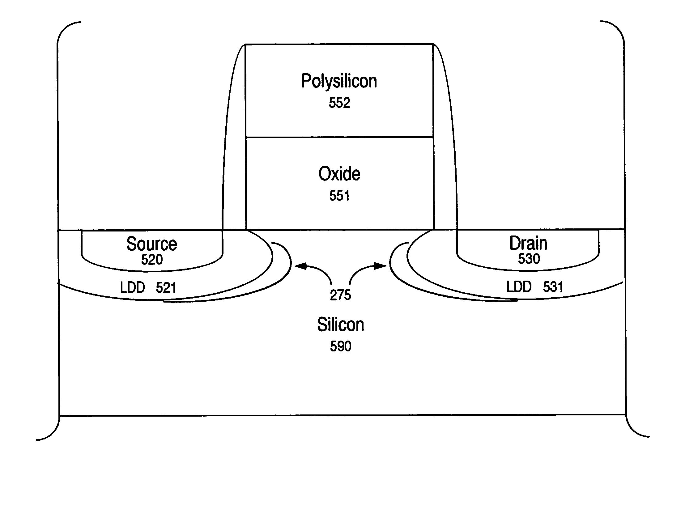
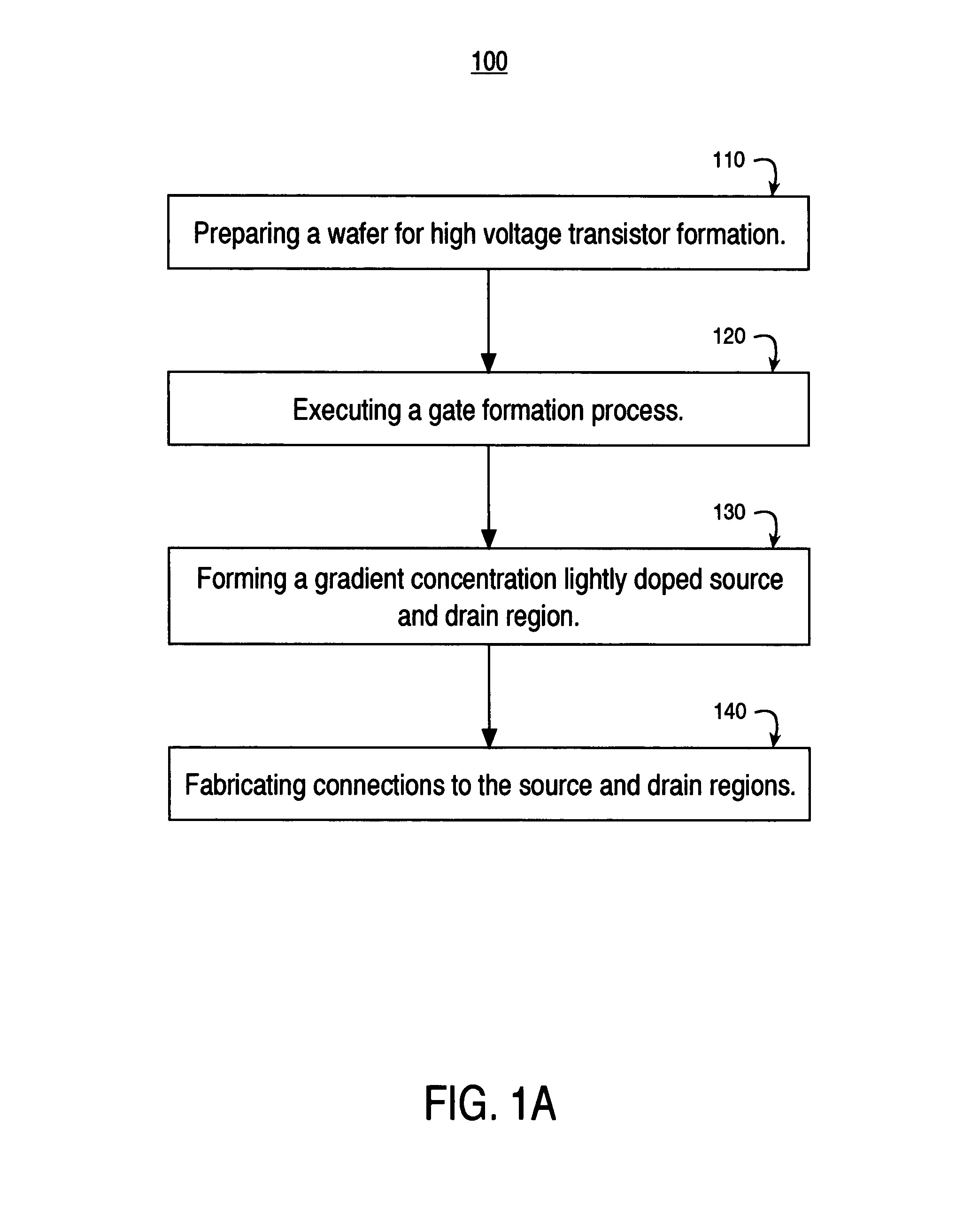
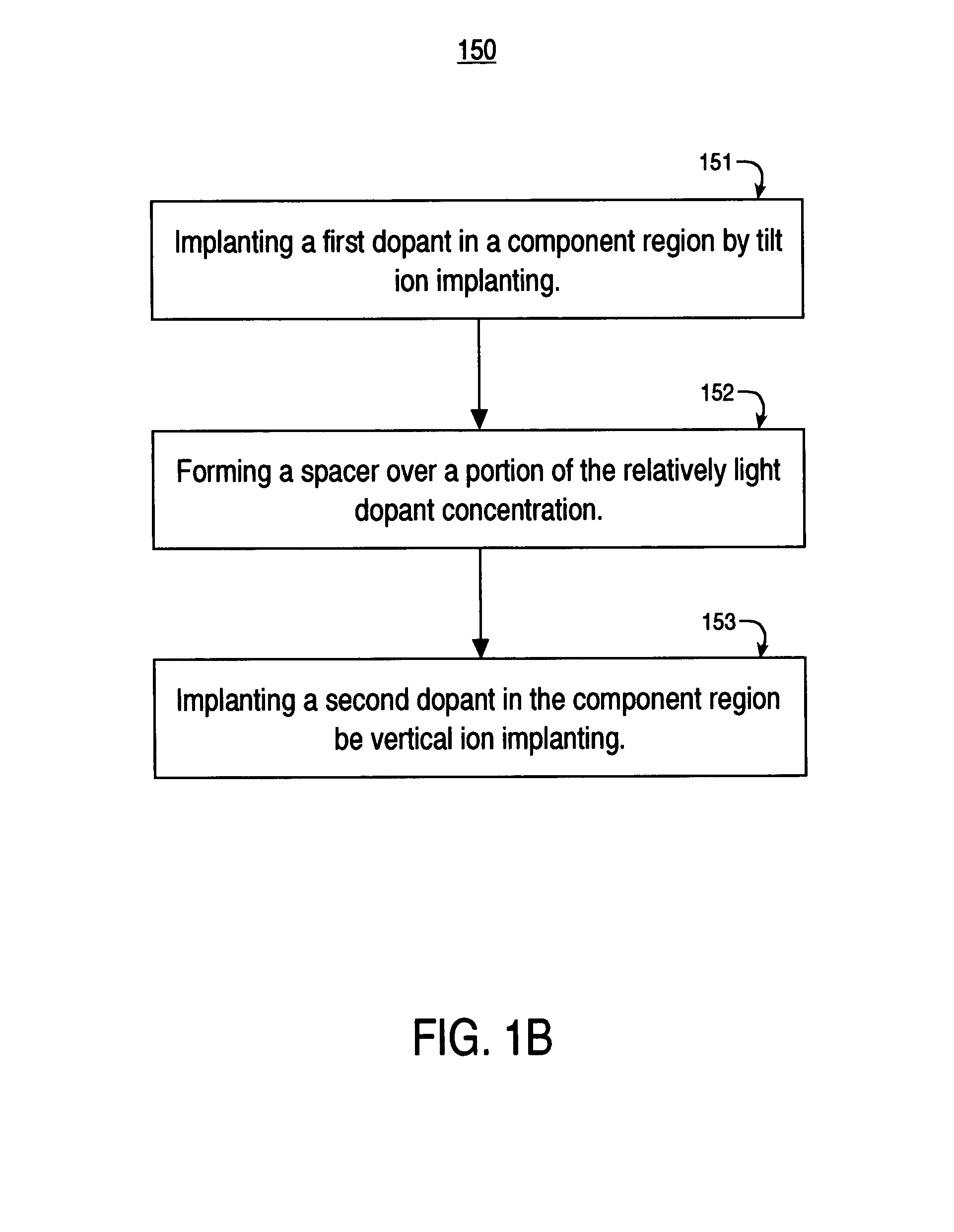
[0017]Reference will now be made in detail to the preferred embodiments of the invention, examples of which are illustrated in the accompanying drawings. While the invention will be described in conjunction with the preferred embodiments, it will be understood that they are not intended to limit the invention to these embodiments. On the contrary, the invention is intended to cover alternatives, modifications and equivalents, which may be included within the spirit and scope of the invention as defined by the appended claims. Furthermore, in the following detailed description of the present invention, numerous specific details are set forth in order to provide a thorough understanding of the present invention. However, it will be obvious to one ordinarily skilled in the art that the present invention may be practiced without these specific details. In other instances, well known methods, procedures, components, and circuits have not been described in detail as not to unnecessarily o...


PUM


Abstract

The present invention is a high voltage transistor formation method and system that includes a varying or gradient concentration lightly doped drain and source implant region. The lightly doped drain (LDD) implant region has gradient concentration characteristics that provide a higher concentration under a source and drain and lower concentration close to a surface source drain channel formation under a gate. A lightly doped drain tilt implant process is utilized to form a component area (e.g., a transistor source and/or drain area) with gradient doping profiles. The varying concentration profile provides a smooth electrical characteristic transformation between regions that reduces the probability of hot electron generation otherwise associated with electrical fields that cross abrupt changes between different conductivity orientation regions. The higher concentration of the light dopants at the bottom of the source and drain regions also helps reduce the probability of deep junction breakdown.

Description

TECHNICAL FIELD[0001]The present claimed invention relates to the field of transistor fabrication. More particularly, the present invention relates to a high voltage transistor fabrication system and method that utilizes a tilt ion implant to form a concentration gradient in the source and drain regions.BACKGROUND ART[0002]Electronic systems and circuits have made a significant contribution towards the advancement of modern society and are utilized in a number of applications to achieve advantageous results. Numerous electronic technologies such as digital computers, calculators, audio devices, video equipment, and telephone systems have facilitated increased productivity and reduced costs in analyzing and communicating data, ideas and trends in most areas of business, science, education and entertainment. Electronic systems designed to produce these results often comprise integrated circuits fabricated on semiconductor chips. Transistors are one of the most prolific basic building ...

Claims


Application Information

Patent Timeline
IPC IPC(8): H01L21/336H01L21/8234
CPCH01L21/26586H01L29/7836H01L29/7833H01L29/6659
Inventor JU, DONG-HYUKWONG, NGA-CHING ALAN
Owner CYPRESS SEMICON CORP
Why Eureka
Try Eureka