Method to improve etching of resist protective oxide (RPO) to prevent photo-resist peeling

a technology of resist protective oxide and etching method, which is applied in the direction of basic electric elements, electrical apparatus, semiconductor devices, etc., can solve the problems of resist peeling, mask lift-off, poor dimensional control and resist mask peeling, and resist peeling problems that are even more severe, and achieve the effect of preventing the peeling of the photo-resist mask

Inactive Publication Date: 2006-03-21
TSMC CHINA COMPANY
View PDF13 Cites 24 Cited by
  • Summary
  • Abstract
  • Description
  • Claims
  • Application Information

AI Technical Summary

Benefits of technology

[0011]It is yet another objective to describe a resist protective oxide etching process that prevents peeling of the photo-resist mask during RPO patterning.

Problems solved by technology

RPO etching process is critical, depending upon the application since other oxide films in the unmasked areas of the chip get attacked as well.
When wet etching is used, the process will produce undercut profiles near the edge of the resist mask, resulting in poor dimensional control and resist mask peeling and mask lift-off.
Resist peeling problems become even more severe as the ground rule dimensions (e.g. line width and spacing) shrink to less than 0.25 μm, with large sections on the wafer floating off during the rinsing step following the etching step.
However, patterning of RPO is not the main objective of these patents.
No solutions are proposed in these references on overcoming the disadvantages related to RPO patterning by the single step wet etching or dry etching processes in the prior art.

Method used


Image

  • Method to improve etching of resist protective oxide (RPO) to prevent photo-resist peeling
  • Method to improve etching of resist protective oxide (RPO) to prevent photo-resist peeling
  • Method to improve etching of resist protective oxide (RPO) to prevent photo-resist peeling

Examples


Embodiment Construction

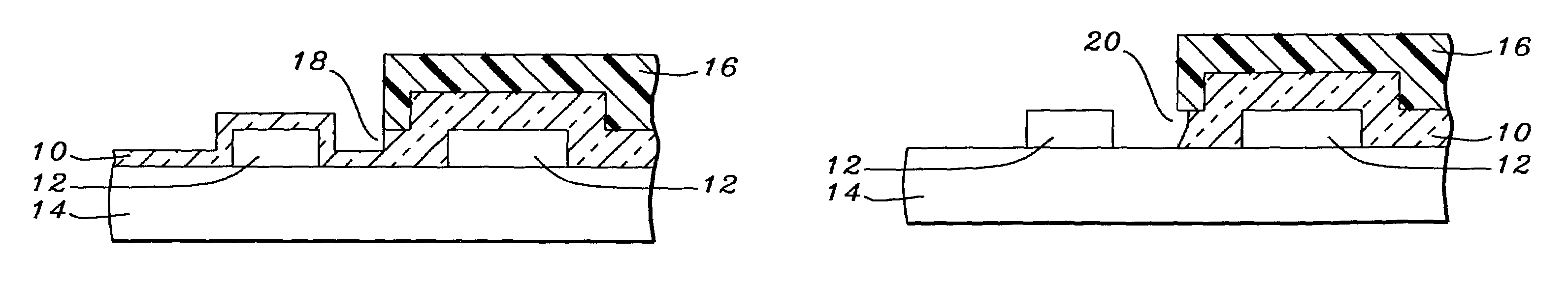
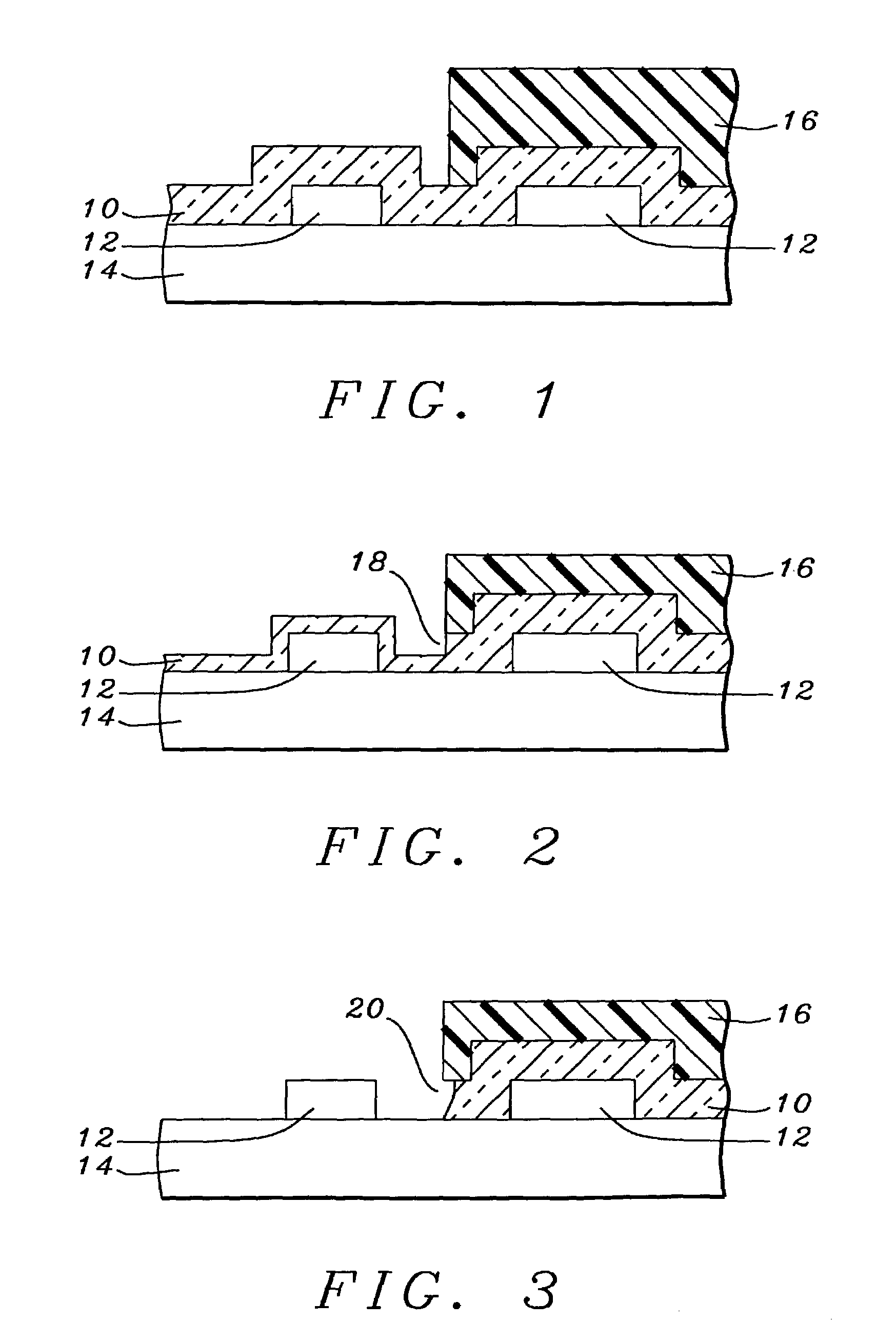
[0023]Although the process of the invention is and can be used wherever and whenever RPO film is used in the fabrication of a semiconductor device, the invention is described here using an application where logic and memory components are fabricated on the same chip. In this application, electrical contacts are formed in the logic part using self-aligned silicide or salicide contacts; and in the memory part of the chip, these contacts are formed using contact holes etched to the diffused regions of silicon.

[0024]A resist protective dielectric film 10, which is preferably silicon dioxide, is deposited over device components 12 formed in a chip on a silicon substrate 14. Examples of alternate dielectric films that can be used are silicon nitride, silicon oxy-nitride, oxygen-doped silicon nitride, and / or nitrided oxides. Resist mask 16 is then formed over the part of the chip that needs protection from subsequent process steps. The structure is shown in FIG. 1.

[0025]The RPO layer 10 is...


PUM

PropertyMeasurementUnit
thicknessaaaaaaaaaa
widthaaaaaaaaaa
thicknessaaaaaaaaaa

Abstract

An improved method of patterning resist protective dielectric layer and preferably protective silicon dioxide layer is described. The method consists of two sequential etching steps, the first one being a timed plasma etching process and the second one being a timed wet etching process. Plasma etching is used to remove approximately 70%–90% of the RPO film thickness and wet etching is used to remove the remaining 10%–30% of the film thickness. The two-step etching process achieves superior dimensional control, a non-undercut profile under the resist mask and prevents resist mask peeling from failure of adhesion at the mask / RPO film interface. The improved method has wide applications wherever and whenever RPO film is used in the process flow for fabricating semiconductor devices.

Description

BACKGROUND OF THE INVENTION[0001](1) Field of the Invention[0002]The present invention generally relates to etching of resist protective dielectric layer and specifically a protective silicon dioxide layer in the fabrication of a semiconductor device, that may be logic, memory, or a combination thereof.[0003](2) Description of the Prior Art[0004]During the fabrication of a semiconductor device, parts of the device need to be protected while some other parts are processed. When, for example, memory and logic devices are fabricated on the same chip, electrical contacts on the logic part are made using the salicide (self aligned silicide) process. To enable the selective salicidation of the logic side components, the memory part of the chip is protected by resist protective oxide (RPO) and masked with a resist mask. Another example is the fabrication of a chip with a field effect transistor (FET) device and I / O circuitry provided on the same chip. While forming electrical contacts to t...

Claims


Application Information

Patent Timeline
Patent Type & Authority Patents(United States)
IPC IPC(8): H01L21/8242H01L21/033H01L21/285H01L21/311H01L21/8234H01L21/8239H01L27/105
CPCH01L21/0337H01L21/28518H01L21/31105H01L27/1052H01L21/823425H01L21/823475H01L27/105H01L21/31116H10B99/00
Inventor HSU, JYH-SHIOUHSIN, PIN-YIHUANG, CHUAN-CHIEH
Owner TSMC CHINA COMPANY
Why Eureka
Try Eureka