Turning tool for grooving polishing pad, apparatus and method of producing polishing pad using the tool, and polishing pad produced by using the tool

a polishing pad and turning tool technology, applied in the field of turning tools, can solve the problems of uneven polishing, uneven surface wear, uneven polishing, etc., and achieve the effects of high accuracy, easy entry of the drill bit, and increased degree of freedom in processing the bas

Inactive Publication Date: 2006-03-28
TOHO ENG CO LTD
View PDF42 Cites 14 Cited by
  • Summary
  • Abstract
  • Description
  • Claims
  • Application Information

AI Technical Summary

Benefits of technology

[0013]It is therefore a first object of the invention to provide a novel turning tool for cutting circumferential grooves, e.g., a multiplicity of generally concentric annular grooves into a surface of a polishing pad formed of a resin material and utilized for polishing semiconductor devices. The turning tool is capable of forming the fine circumferential grooves with a sufficiently small width and with high dimensional accuracy and high stability. The turning tool enables to form the small-width circumferential grooves in the radially inner portion of the polishing surface of the polishing pad, with ease.
[0014]It is a second object of the invention to provide a novel method of producing a polishing pad formed of a resin material and usable for polishing semiconductor devices, by utilizing a special turning tool constructed according to the present invention. The method enables to form circumferential grooves, e.g., a multiplicity of generally concentric annular grooves on a surface of the polishing pad with a sufficiently small width and with high dimensional accuracy and high stability, over a sufficiently wide area of the surface of the polishing pad including a radially inner portion of the surface of the polishing pad.
[0015]It is a third object of the invention to provide a polishing pad formed of a resin material and usable for polishing semiconductor devices, which is novel in construction, which is suitably produced by using a special turning tool specific working tool constructed according to the present invention, and which is effectively usable for chemical mechanical polishing of a substrate of multilevel interconnection structure in which a width of a metallic interconnection is set to about 0.1 μm.

Problems solved by technology

After a number of polishing runs, the polishing pad having the pattern of recesses may suffer from variation of diameter of the recesses, whereby the pad suffers from difficulty in exhibiting a desired chemical mechanical polishing effect with high stability.
In the case of the polishing pad having the pattern of checked grooves, a polishing condition is likely to vary in the radial direction of the polishing pad, whereby the pad suffers from a high tendency of occurrence of uneven wearing of its surface, resulting in uneven polishing.
However, the disclosed polishing pad suffers from inherent structural problems, namely, difficulty in forming grooves extending in a circumferential direction in the polishing pad and difficulty in ensuring a sufficient dimensional accuracy of the grooves.
In the former case, each of the formed annular grooves is prone to have a dull shape, especially at its open-end edge portions, so that the width of the groove varies in its depth direction.
This causes undesirable variation of the groove width, especially when the polishing surface of the polishing pad is worn or is conditioned by the dressing process, resulting in unstable polishing conditions.
In the latter case, since the annular grooves are formed by milling of the saw blade on the mill, the formed annular grooves is likely to extend straightly to some extent, making it difficult to form a groove having a small width and a small radius of curvature.
This makes it impossible to form a desired polishing pad in which annular grooves having a relatively small width are formed on a radially inner portion of its polishing surface as well as a radially intermediate and a radially outer portion of its polishing surface.
In view of a recent tendency of employing a large-diameter wafer, e.g., a wafer having a diameter within a range of 200 mm–300 mm or more, the presence of useless area in the radially inner portion of the polishing surface of the polishing pad undesirably causes an enlargement in size of the polishing pad.
Therefore, the problem of the radially inner useless area of the polishing pad becomes very significant.
However, since the polishing pad is formed of a specific material having somewhat elasticity, e.g., a foamed rigid-resin material, it is significantly difficult to cut an annular groove having a relatively small width and having a relatively small radius of curvature into the polishing pad, with high dimensional accuracy.
In the light of the physical property of the polishing pad, conventionally available tool for cutting a work piece made of metal or a rigid-resin material, are not suitable to cut the polishing pad.
For instance, the tools for cutting the metallic or rigid-resin working piece are likely to interfere with the walls of each groove, thereby possibly producing burrs or other defects in the walls of the grooves.
Thus, the conventionally available tools are incapable of cutting the small-width and small-radius grooves into the surface of the polishing pad having the somewhat elasticity, like the foamed rigid-resin members.
Thus, the conventional polishing pad disclosed in the above U.S. Patents is insufficient for ensuring currently required polishing accuracy and polishing efficiency, and accordingly is unsuitable to be used for CMP for a planarization of a currently developed substrate of multilevel interconnection, which includes interconnect metal layers made of a soft cupper or gold.
However, this surface deformation mechanism of the conventional polishing pad is insufficient to keep pace with the currently required level of polishing accuracy.
In addition, the use of the backside pad, which is formed differently from the polishing pad, evidently has pushed up a manufacturing cost of the polishing pad.

Method used


Image

  • Turning tool for grooving polishing pad, apparatus and method of producing polishing pad using the tool, and polishing pad produced by using the tool
  • Turning tool for grooving polishing pad, apparatus and method of producing polishing pad using the tool, and polishing pad produced by using the tool
  • Turning tool for grooving polishing pad, apparatus and method of producing polishing pad using the tool, and polishing pad produced by using the tool

Examples


examples

[0169]To further illustrate the present invention, there will be described some examples of the invention. It is to be understood that the invention is not limited to the details of these examples, but may be embodied with various changes, modifications and improvements, which may occur to those skilled in the art, without departing from the spirit and scope of the invention defined in the appended claims.

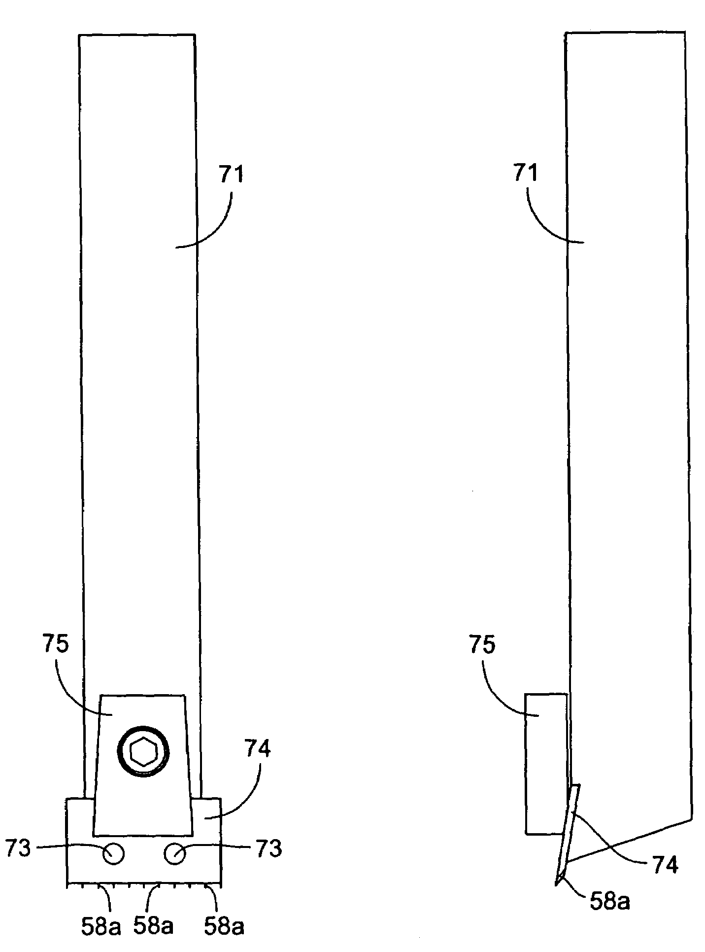
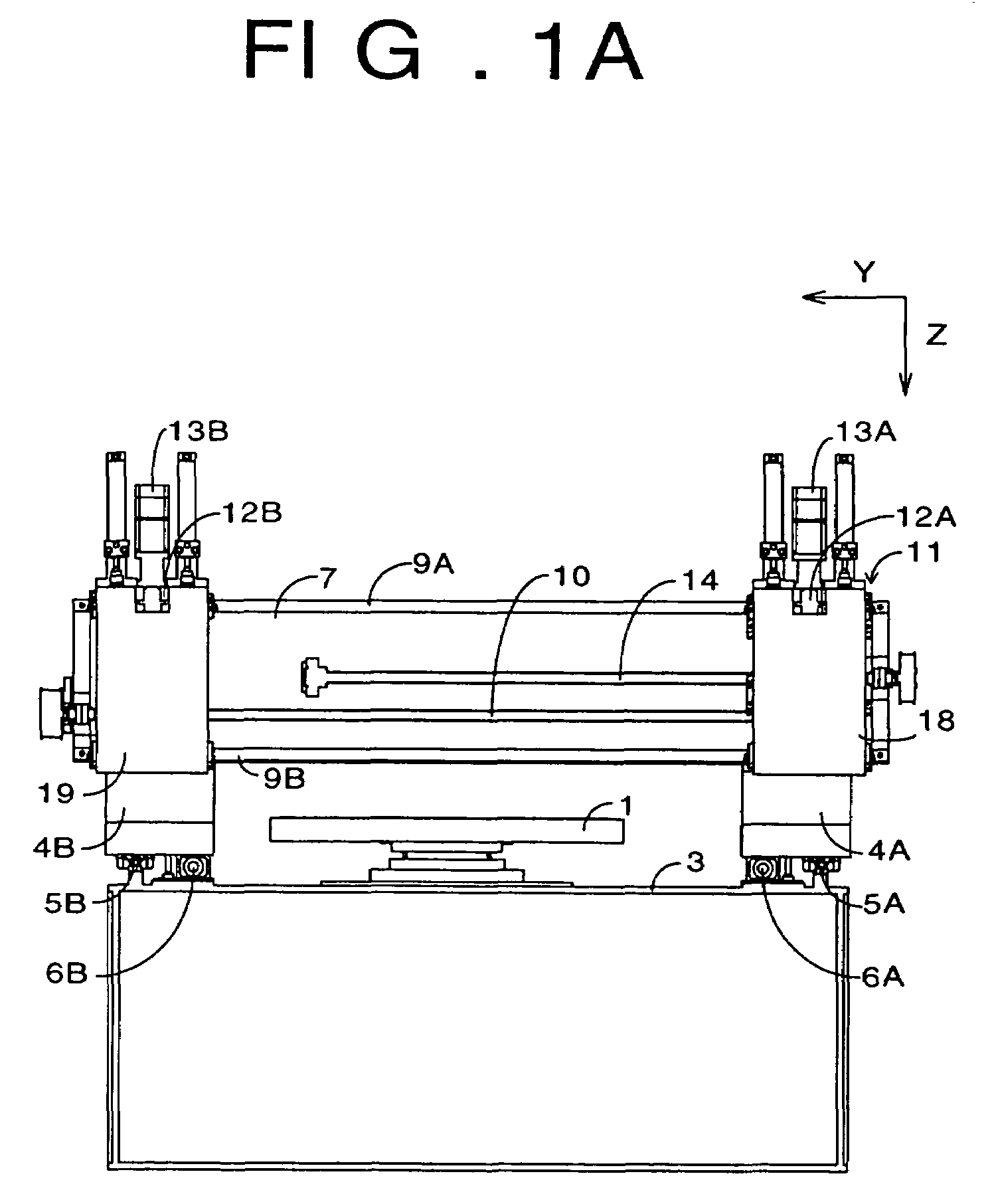
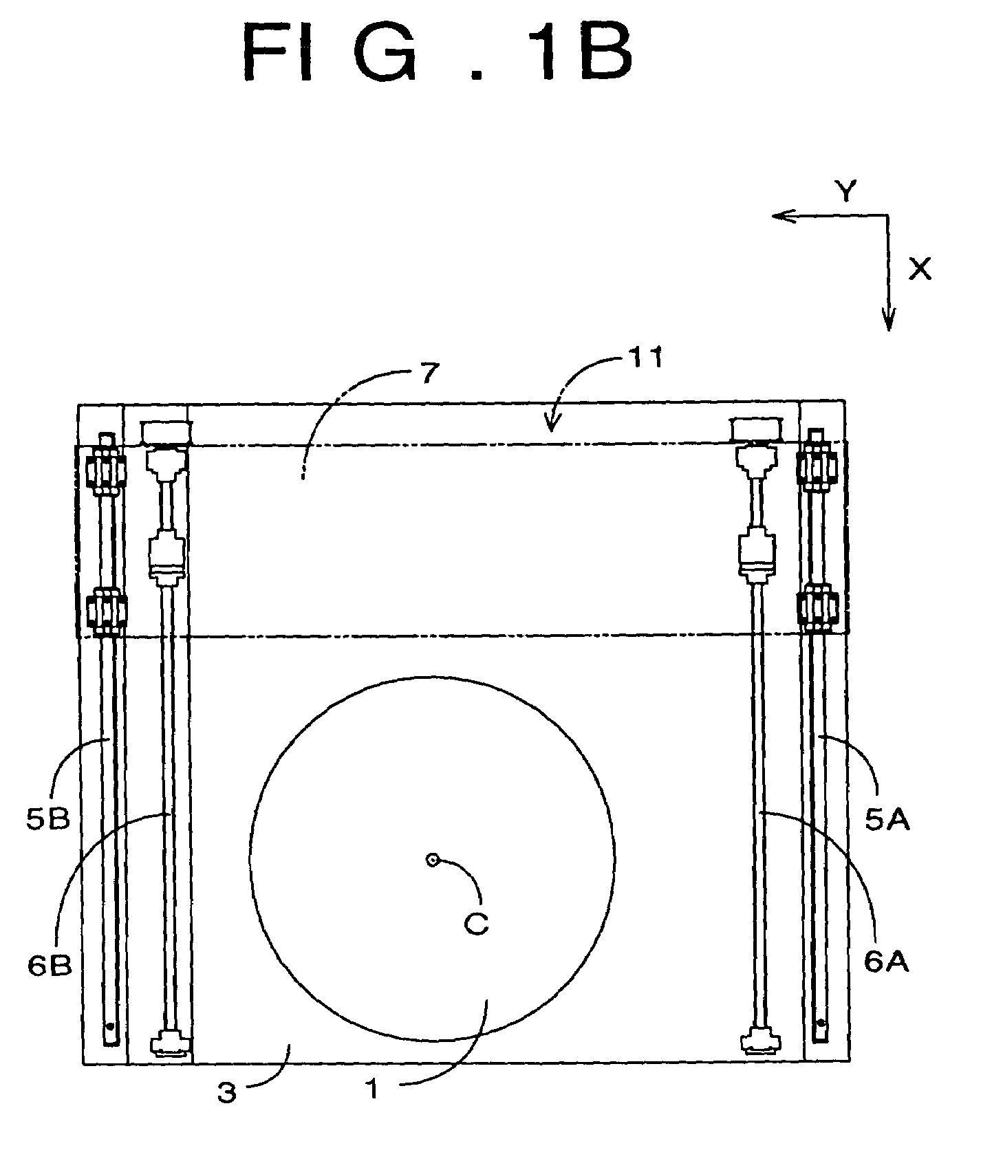
[0170]There were prepared two specimens of the polishing pad according to Examples 1 and 2 of the present invention as shown in FIGS. 30, 31 by cutting multiplicity of generally concentric annular grooves 130 into surfaces of respective foamed urethane pads 15 by using respective multi-edged tools 74 each constructed according to the present invention as indicated in the following Table 1. Described in detail, each of the specimens of Examples 1 and 2 is formed by using the grooving machine of the present invention. The foamed urethane pad 15 attracted on the suction plate 16 of th...


PUM

PropertyMeasurementUnit
angleaaaaaaaaaa
angleaaaaaaaaaa
rake angleaaaaaaaaaa

Abstract

Disclosed is a turning tool for cutting circumferential grooves into a surface of a polishing pad formed of a resin material and utilized for polishing semiconductor devices. The turning tool comprising a cutting part arranged to have a tooth width within a range of 0.005–1.0 mm, a wedge angle within a range of 15–35 degrees, and a front clearance angle within a range of 65–45 degrees. A polishing pad effectively formed by using the turning tool, and an apparatus and a method of producing such a polishing pad by utilizing the turning tool are also disclosed.

Description

[0001]This is a Division of application Ser. No. 10 / 026,504 filed Dec. 19, 2001.BACKGROUND OF THE INVENTION[0002]1. Field of the Invention[0003]The present invention relates to a turning tool for producing a polishing pad made of a resin material and usable in the fabrication of semiconductor devices, especially for chemical mechanical polishing (CMP) executed for planaraizing surfaces of semiconductor wafers or devices. The present invention further relates to a polishing pad effectively formed by using the turning tool, and an apparatus and a method of producing such a polishing pad by utilizing the turning tool.[0004]2. Description of the Related Art[0005]In the semiconductor fabrication processes, a substrate, e.g., a silicon wafer, may undergo multiple masking, etching, implantation, and dielectric and conductor deposition processes, to thereby form a lamination of various kinds of thin layers such as metallic layers and insulative layers. Between each processing steps, it is u...

Claims


Application Information

Patent Timeline
Patent Type & Authority Patents(United States)
IPC IPC(8): B23P13/00B23B27/04B23B27/16B23C5/08B23C5/10B23Q1/52B23Q16/04B24B37/26B24D13/14B24D18/00
CPCB23B27/04B23C5/08B23C5/10B23Q1/52B23Q16/04B24B37/26B24D18/00Y10T407/2208B23B2210/022B23B2220/12B23B2251/50Y10T407/23Y10T407/2206Y10T29/49995Y10T407/2202Y10T29/5168Y10T82/10Y10T407/25B23B2210/02Y10T83/0304B23B2251/043B23B2260/0482
Inventor SUZUKI, TATSUTOSHI
Owner TOHO ENG CO LTD
Why Eureka
Try Eureka