
Fabrication method, varactor, and integrated circuit

a varactor and varactor technology, applied in the field of silicon ictechnology, can solve problems such as insufficient integration, and achieve the effects of high q value, good performance and high sensitivity

Inactive Publication Date: 2006-04-11
INFINEON TECH AG
View PDF9 Cites 7 Cited by
  • Summary
  • Abstract
  • Description
  • Claims
  • Application Information

AI Technical Summary

Benefits of technology

The method produces a varactor with a linear voltage-frequency response, enhanced sensitivity, and a high quality factor, facilitating easier noise minimization and improved performance in VCOs, especially in bipolar integrated circuits for radio frequency applications.

Problems solved by technology

U.S. Pat. No. 5,405,790 does not teach how to select or control the doping profile / CV-characteristics of the varactor, and the circuit of U.S. Pat. No. 5,477,197 is not fully integratable as, inter alia, a crystal oscillating element is used.

Method used


Image

  • Fabrication method, varactor, and integrated circuit
  • Fabrication method, varactor, and integrated circuit
  • Fabrication method, varactor, and integrated circuit

Examples


Embodiment Construction

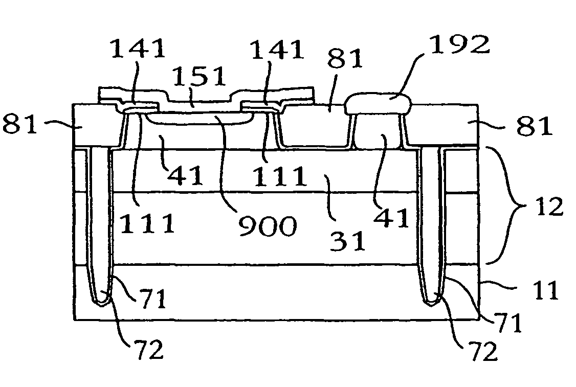
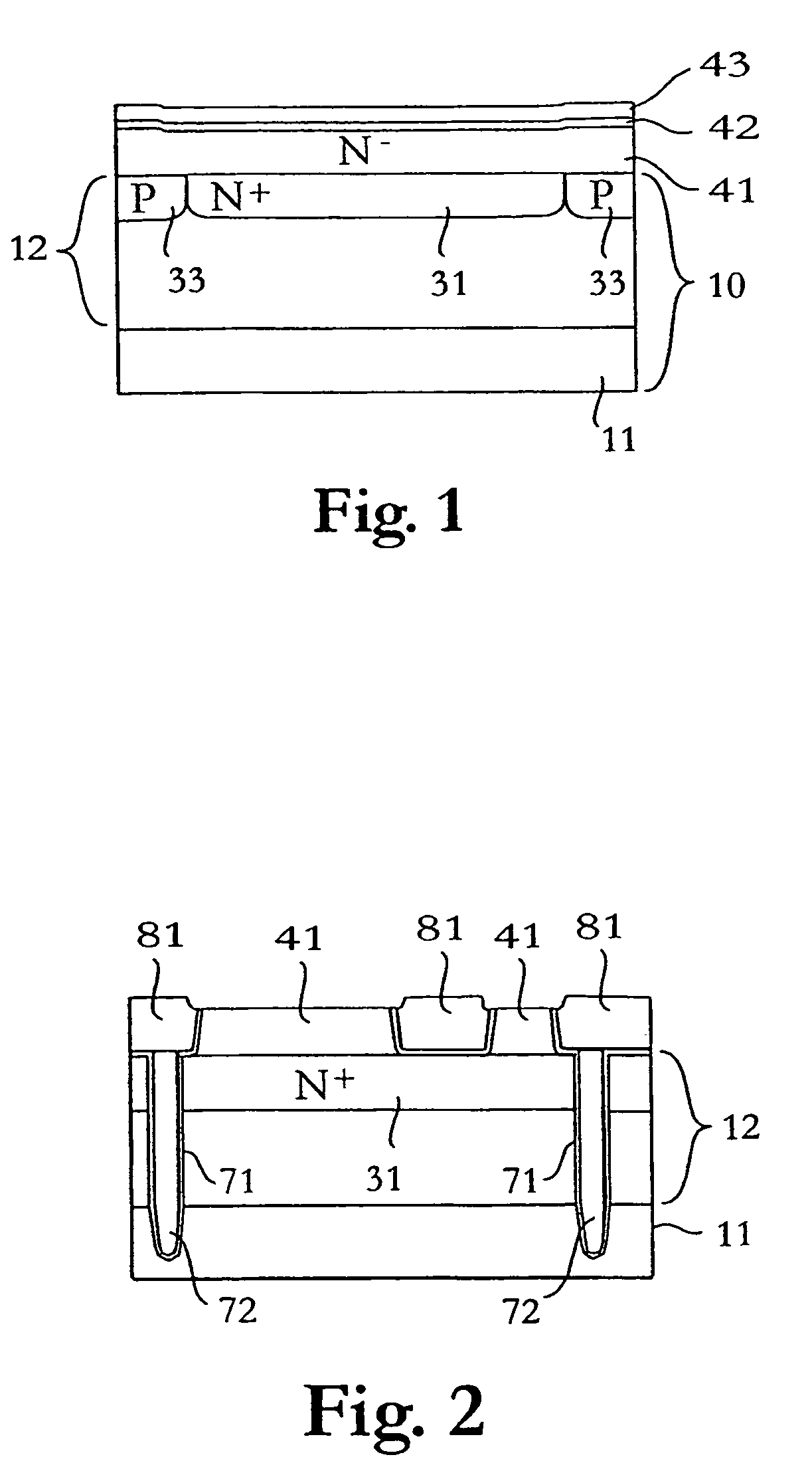
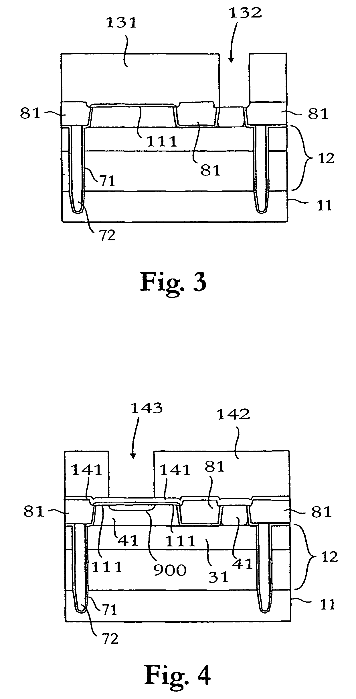
[0043]A method of manufacturing a varactor of the present invention in a bipolar process, to which only a few specific process steps are added, is overviewed below with reference to FIGS. 1–6.

[0044]To reach a structure as the one illustrated in FIG. 1 a starting material 10 consisting of a highly p+-doped wafer 11 is provided, on which a low-doped epitaxial silicon layer 12 of p-type is grown. Alternatively, the p-type wafer can be a homogeneously low-doped p-type wafer (not illustrated).

[0045]In the surface of the layer 12 buried n+-doped 31 and p-doped 33 regions are formed by means of (i) forming a thin protective layer of silicon dioxide (not illustrated) on the layer 12; (ii) forming a mask thereon by photolithographic methods to define the region for the n+-doped regions 31 (of which only one is shown in FIG. 1); (iii) n+-type doping the regions 31 defined by the mask; (iv) removing the mask; (v) heat treating the structure obtained; (vi) p-type doping the structure to obtain ...


PUM


Abstract

A method in the fabrication of an integrated bipolar circuit for forming a p / n-junction varactor is disclosed. The method featuring the steps of providing a p-doped substrate (10; 10, 41); forming a buried n+-doped region (31) in the substrate; forming in the substrate an n-doped region (41) above the buried n+-doped region (31); forming field isolation (81) around the n-doped region (41); multiple ion implanting the n-doped region (41); forming a p+-doped region (151) on the n-doped region (41); forming an n+-doped contact region to the buried n+-doped region (31), the contact region being separated from the n-doped region (41); and heat treating the hereby obtained structure to set the doping profiles of the doped regions. The multiple ion implantation of the n-doped region (41); the formation of the p+-doped region (151); and the heat treatment are performed to obtain a hyper-abrupt p+ / n-junction within the n-doped region (41).

Description

CROSS REFERENCE TO RELATED APPLICATION[0001]This application is a continuation of copending International Application No. PCT / SE03 / 00048 filed Jan. 15, 2003 which designates the United States, and claims priority to Swedish application no. 0200137-8 filed Jan. 18, 2002.TECHNICAL FIELD OF THE INVENTION[0002]The present invention generally relates to the field of silicon IC-technology, and more specifically the invention relates to the formation of a varactor in a semiconductor bipolar or BiCMOS process flow; to the varactor formed, and to a voltage controlled oscillator (VCO).DESCRIPTION OF RELATED ART AND BACKGROUND OF THE INVENTION[0003]Advanced silicon bipolar, CMOS or BiCMOS circuits are used today for high-speed applications in the 1–5 GHz frequency range, replacing circuits previously only possible to realize using III–V based technologies.[0004]A common trend in microelectronics is to integrate more and more functions on a single chip, in order to increase the general performa...

Claims


Application Information

Patent Timeline
Patent Type & Authority Patents(United States)
IPC IPC(8): H01L21/20H01L29/93
CPCH01L29/93
Inventor JOHANSSON, TEDNORSTROM, HANSSAHL, STEFAN
Owner INFINEON TECH AG
Learn More