Method and apparatus for distributed synchronous clocking

a synchronous clocking and distributed technology, applied in the field of methods and apparatuses, can solve the problems of power requirements and transmission line effects of high-speed clock signals that are not suited to the power requirements of high-speed clock signals, and the jitter of clocking signals along these paths becomes an ever increasing problem, and the effect of power requirements and transmission lines

Inactive Publication Date: 2006-04-25
MCGILL UNIV
View PDF20 Cites 29 Cited by
  • Summary
  • Abstract
  • Description
  • Claims
  • Application Information

AI Technical Summary

Benefits of technology

[0010]It is an object of the present invention to overcome, or at least mitigate, the shortcomings of the known clocking arrangements and to provide a method and apparatus for synchronizing clocking at distributed nodes in synchronized electronic, optical or optoelectronic systems, such as computing or switching systems.
[0018]The method may further comprise, at each slave node, the step of adjusting delay units in each propagation channel, when the phase difference is greater than the preset level, so as to reduce the phase difference between subsequently-arriving pairs of pulses.
[0027]Each of the pre-delay units and post-delay units may comprise a plurality of delay elements and the slave nodes may each have means for increasing the number of delay elements active in one of the delay units and decreasing the number of active delay elements in the other of the delay units correspondingly.

Problems solved by technology

As the speed of operation increases, however, primarily due to the reduction in transistor size, the skew and jitter of clocking signals along these paths becomes an ever increasing problem for the register-based architectures of most existing computing systems.
Clock-skew is especially problematic when the system exceeds a certain size, nominally when the delay paths become longer than a couple of centimeters.
The power requirements and the transmission line effects for high-speed clock signals are not suited for standard printed-circuit board (PCB) layouts and typically limit the speed of operation to less than 100 MHz.
These difficulties are compounded by the noise and coupling of multiple parallel data buses operating in unison on typical computing PCBs.
These contribute latency to the communication as well as lead to a greater amount of circuitry.
However, this type of clocking structure is often difficult to calibrate.
Great care must be used when cutting and connecting the wires of a T-branch to ensure that they are precisely the same length; otherwise the mismatch will cause the travelling pulses to arrive at their destinations at slightly different times, thus causing skew in the clocks.
The most significant drawback to this design is the susceptibility of both the amplifiers and the connecting wires to environmental effects, such as temperature and time degradation.
These methods are generally complex and assume that the electrical characteristics of the transmission medium never change.
Moreover, the arrangements cannot correct for any possible speeding-up or slowing-down in segments of the transmission line due to thermal variations, dielectric variations or other factors which can change propagation velocity within the medium.

Method used


Image

  • Method and apparatus for distributed synchronous clocking
  • Method and apparatus for distributed synchronous clocking
  • Method and apparatus for distributed synchronous clocking

Examples


Embodiment Construction

[0038]In the drawings, corresponding items in the different Figures have the same reference numbers.

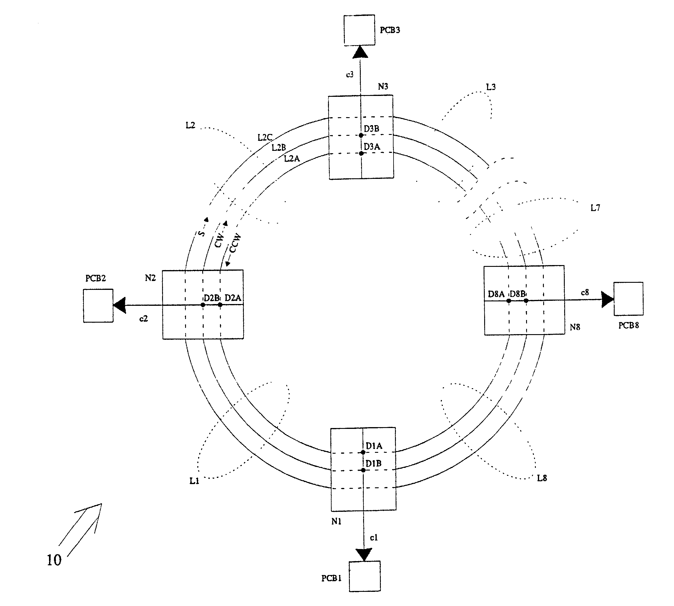
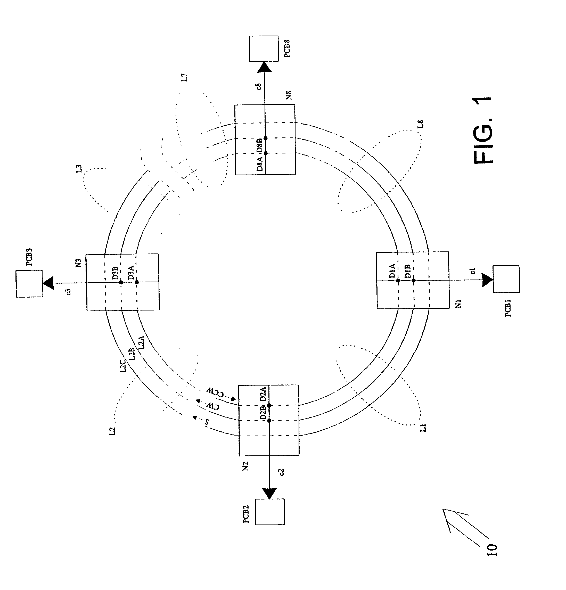
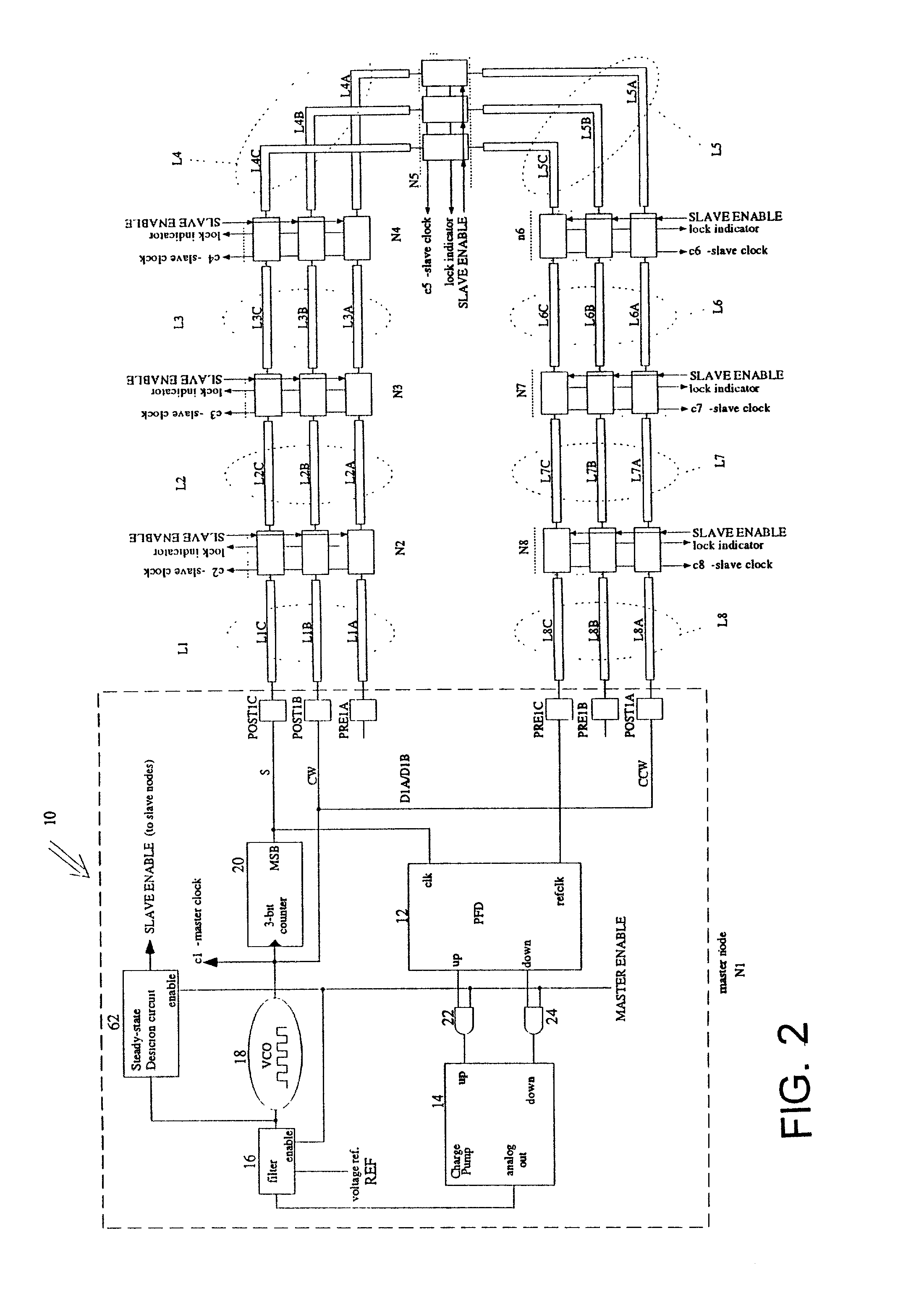
[0039]FIGS. 1 and 2 illustrate, schematically, a high-speed synchronous digital system 10, such as a computing or communications switching system, having a plurality of nodes N1 . . . N8 interconnected by propagation channels L1 . . . L8 for clock synchronization pulses. Node N1 comprises a master node and nodes N2 . . . N8 comprise slave nodes. For ease of illustration, only four of the nodes, N1, N2, N3 and N8, are shown in FIG. 1. It should be appreciated that the invention is not limited to systems having only eight nodes, however; a practical system could have many more nodes. The nodes N1, N2, N3, . . . N8 are associated with system parts whose operations are synchronized by clock signals c1, c2, c3, . . . c8, supplied by nodes N1, N2, N3, . . . N8, respectively. These system parts are represented as printed circuit boards PCB1, PCB2, PCB3, . . . PCB8, respectively, but it shoul...


PUM


Abstract

A method and an apparatus are provided for synchronizing clock signals in spatially distributed nodes in large, synchronous electronic, optical, optoelectronic or wireless systems, such as systems comprising arrays of microprocessors and memories, and telecommunication systems. The nodes comprise a master node and a plurality of slave nodes. The master node generates first and second identical pulse trains and propagates them to the slave nodes via a first and second propagation channels, respectively, so that a pair of pulses, one from each pulse train, arrive at each slave node substantially simultaneously, travelling in opposite directions. Each slave node generates a clock signal event in response to the substantially simultaneous arrival of each pair of pulses. The master node maintains the rate of the two pulse trains such that there are “pN” pulses in each propagation channel at any time, where “N” is the number of nodes and “p” is an integer. Adjustable delays are provided at each slave node, disposed in each propagation channel. When the pulses in the two channels do not arrive simultaneously, the slave node adjusts the delay units so as reduce differences in the arrival times of subsequent pairs of pulses. The delay units may comprise pre-delay units upstream of the detection point and post-delay unit downstream of the detection point, any increment in a pre-delay being compensated by an equal decrement in the post-delay in the same propagation channel.

Description

[0001]This application claims priority from U.S. provisional patent application No. 60 / 179,751 filed Feb. 02, 2000.FIELD OF INVENTION[0002]The invention relates to a method and apparatus for providing synchronous clocking, and is especially applicable to synchronous clocking systems for spatially distributed nodes in large synchronous electronic, optical or optoelectronic systems. These can include computational systems that comprise arrays of microprocessors and memories, as well as telecommunication systems that must switch large amounts of data.BACKGROUND OF INVENTION[0003]Hitherto, synchronization techniques of most processing and switching circuitry have entailed the careful layout and the prudent use of many mechanisms such as phase-lock loops and binary-tree signal paths. These mechanisms are used to equalize delay paths to distributed nodes in a chip or system. As the speed of operation increases, however, primarily due to the reduction in transistor size, the skew and jitte...

Claims


Application Information

Patent Timeline
Patent Type & Authority Patents(United States)
IPC IPC(8): H04L12/28H04J3/06H04L27/28
CPCH04J3/0685
Inventor ROLSTON, DAVID ROBERT CAMERONPLANT, DAVID VICTORROBERTS, GORDON WALTER
Owner MCGILL UNIV
Why Eureka
Try Eureka