Front side illuminated photodiode with backside bump

a photodiode and backside technology, applied in the field of semiconductor devices, can solve the problems of increasing the capacitance of the device, complex design of the backside illuminated photodiode, and the performance of the front side illuminated photodiod

Active Publication Date: 2006-05-02
MICROSEMI
View PDF16 Cites 60 Cited by
  • Summary
  • Abstract
  • Description
  • Claims
  • Application Information

AI Technical Summary

Benefits of technology

[0022]For purposes of summarizing the invention, certain aspects, advantages and novel features of the invention have been described herein. It is to be understood that not necessarily all such advantages may be achieved in accordance with any particular embodiment of the invention. Thus, the invention may be embodied or carried out in a manner that achieves or optimizes one advantage or group of advantages as taught herein without necessarily achieving other advantages as may be taught or suggested herein.

Problems solved by technology

The design of a backside illuminated photodiode is complex, and its performance is usually inferior to a front side illuminated photodiode.
A photodiode with a wider aperture may be required to capture all of the light, which will increase the device capacitance and degrade the speed of the device.
Active alignment is time consuming and an expensive assembly technique.
Furthermore, testing a backside-illuminated photodiode is not as easy as testing a front illuminated photodiode.
Sampling tests are done after the chip is mounted in a flip chip package, which adds cost and long cycle time to the testing of the backside illuminated photodiode.
Finally, backside illuminated photodiodes are not feasible using absorptive chip substrates, such as, for example, silicon (Si), germanium (Ge) or gallium arsenide (GaAs) semiconductors.
Although the flip chip package shown in FIG. 2 alleviates some of the problems associated with backside illumination, the hole through the chip carrier 100 imposes more difficulties in the packaging of the photodiode and is not conducive to chip-on-chip packages.

Method used


Image

  • Front side illuminated photodiode with backside bump
  • Front side illuminated photodiode with backside bump
  • Front side illuminated photodiode with backside bump

Examples


Embodiment Construction

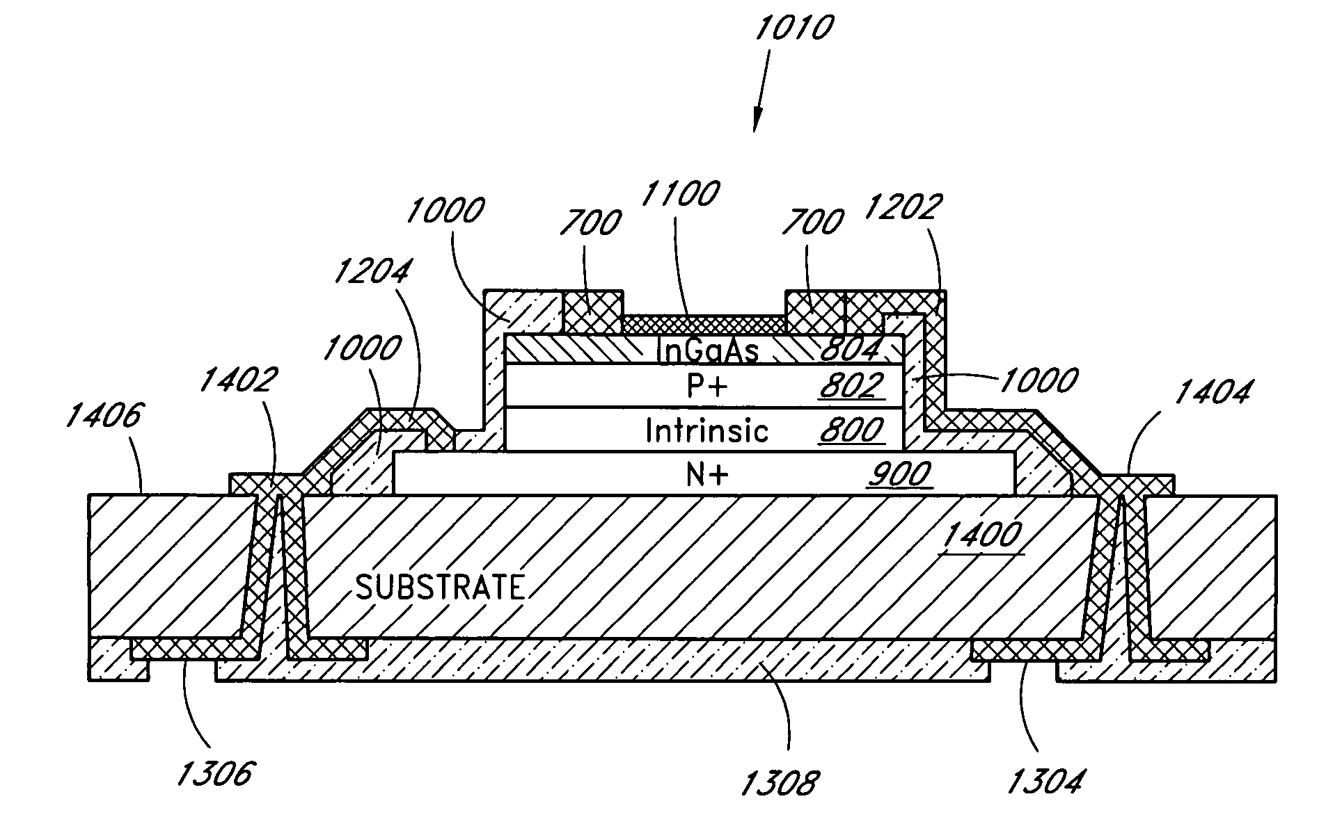
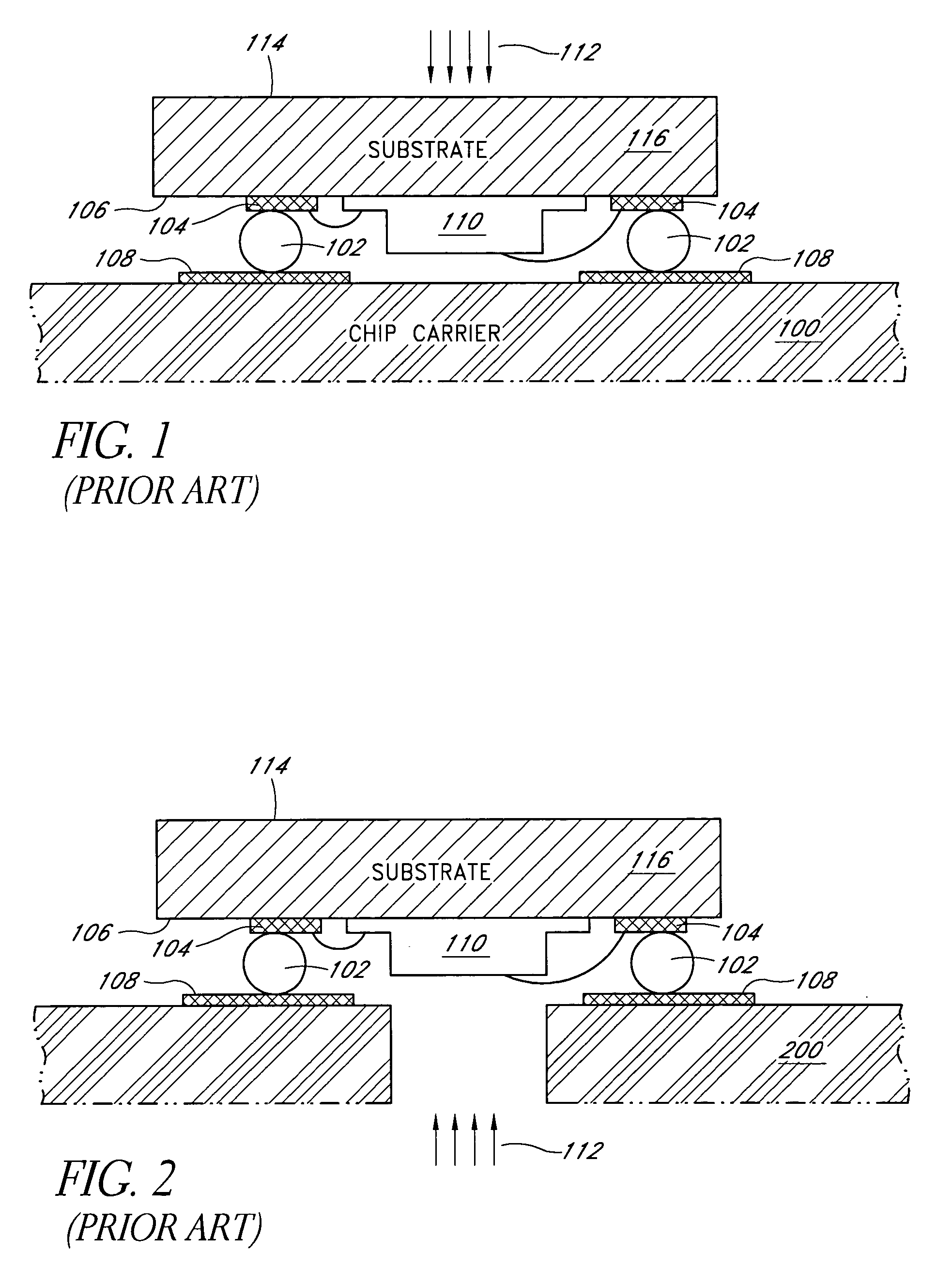
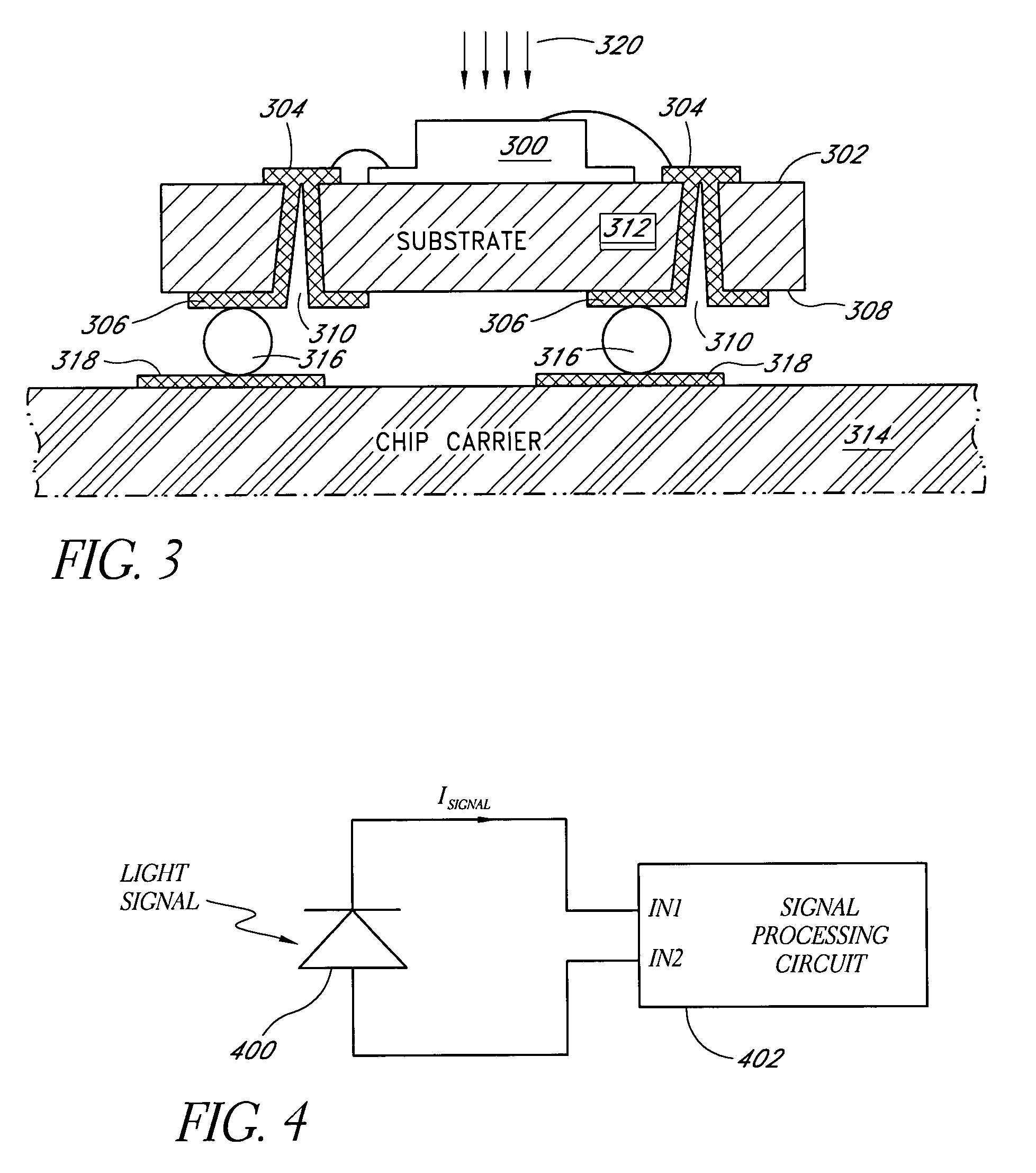
[0030]In the following detailed description of the invention, reference is made to the accompanying drawings which form a part thereof, and in which is shown, by way of illustration, specific embodiments in which the invention may be practiced. In the drawings, like numerals describe similar components throughout the several views.

[0031]In the following description, the terms wafer and substrate are interchangeably used to refer generally to any structure on which integrated circuits (ICs) are formed, and also to such structures during various stages of integrated circuit fabrication. Both wafer and substrate include doped and undoped semiconductors, epitaxial semiconductor layers supported by a base semiconductor or insulator, combinations of such layers, as well as other semiconductor structures well known to one skilled in the art, including bulk semiconductor and semiconductor-on-insulator (SOI) substrates. The term conductor is understood to include semiconductors, and the term...


PUM


Abstract

This invention relates to a novel optoelectronic chip with one or more optoelectronic devices, such as photodiodes, fabricated on a front side of a semiconductor wafer and contacts on a backside of the semiconductor wafer. The backside contacts can be contact bumps, which allow the optoelectronic chip to achieve the benefits of flip chip packaging without flipping the optoelectronic chip upside down with respect to a chip carrier. In an optical communication system, a photodiode chip can be backside bumped to a chip carrier or an electronic chip, allowing front side illumination of the photodiode chip. Front side illumination offers many benefits, including improved fiber alignment, reduced manufacturing time, and overall cost reduction.

Description

RELATED APPLICATION[0001]This application claims the benefit of priority under 35 U.S.C. § 119(e) of U.S. Provisional Application No. 60 / 413,427 entitled “Frontside Illuminated Photodiode With Backside Bump,” filed on Sep. 25, 2002, the entirety of which is incorporated herein by reference.BACKGROUND OF THE INVENTION[0002]1. Field of the Invention[0003]The present invention relates to semiconductor devices and, in particular, refers to an optoelectronic device.[0004]2. Description of the Related Art[0005]Photodiodes are used in optical communication networks to convert optical signals to electrical signals for processing using electronic circuits. In high bandwidth applications, the photodiodes can often be packaged using flip chip interconnections. The flip chip interconnections provide many benefits, including smaller package size, elimination of bond wires, and improved signal integrity.[0006]FIG. 1 illustrates a typical flip chip package for a backside-illuminated photodiode. A ...

Claims


Application Information

Patent Timeline
Patent Type & Authority Patents(United States)
IPC IPC(8): H01L31/00H01L31/0203
CPCH01L31/0203H01L31/105H01L27/1446H01L27/14636H01L2224/48227H01L2224/49107H01L2924/30107H01L2224/48091H01L2924/00014H01L2924/00H01L2924/12032
Inventor LAI, JAY JIEVU, TRUC Q.WARREN, GARY B.
Owner MICROSEMI
Why Eureka
Try Eureka