System supporting multiple memory modes including a burst extended data out mode

a technology of extended data and memory mode, applied in the direction of memory adressing/allocation/relocation, generating/distributing signals, instruments, etc., can solve the problems of data valid for a few nanoseconds, excessively high price, and constant decline in price per bit of these memory devices, so as to achieve fast data access and high speed data access. , the effect of high speed

Inactive Publication Date: 2006-05-09
ROUND ROCK RES LLC
View PDF127 Cites 31 Cited by
  • Summary
  • Abstract
  • Description
  • Claims
  • Application Information

AI Technical Summary

Benefits of technology

[0008]An integrated circuit memory device with a standard DRAM pinout is designed for high speed data access and for compatibility with existing memory systems. A high speed burst mode of operation is provided where multiple sequential accesses occur following a single column address, and read data is output relative to the /CAS control signal. In the burst mode of operation the address is incremented internal to the device eliminating the need for external address lines to switch at high frequencies. Read/Write commands are issued once per burst access eliminating the need to toggle the Read/Write control line at high speeds. Only one control line per memory chip (/CAS) must toggle at the operating frequency in order to clock the internal address counter and the data input/output latches. The load on each /CAS is typically less than the load on the other control signals (/RAS, /WE and /OE) since each /CAS typically controls only a byte width of the data bus. Internal circuitry of the memory device is largely compatible with existing Extended Data Out (EDO) DRAMs. This similarity allows the two part types to be manufactured on one die with a limited amount of additional circuitry. The ability to switch between a standard non-burst mode and a high speed burst mode allows the device to be used to replace standard devices, and eliminates the need to switch to more complex high speed memory devices. Internal address generation provides for faster data access times than is possible with either fast page mode or EDO DRAMs. The high speed operation of this Burst EDO device eliminates the need to interleave memory devices in order to attain a high data throughput. In contrast to the 50 megahertz interleaved memory system described above, the output data from this device will be valid for approximately 15 nanoseconds significantly easing the design of circuitry required to latch the data from the memory. The device is compatible with existing memory module pinouts. Memory modules include, but are not limited to Single In-Line Memory Modules (SIMMs), Multi-Chip Modules

Problems solved by technology

Except for their high volume production, the state of the art manufacturing requirements of these devices would cause them to be exorbitantly priced.
Yet, due to efficiencies associated with high volume production, the price per bit of these memory devices is continually declining.
This high speed circuitry has allowed for faster page mode cycle times. A problem exists in the reading of a DRAM when the device is operated with minimum fast page mode cycle times. /CAS may be low for as little as 15 nanoseconds, and the data access time from /CAS to valid output data (tCAC) may be up to 15 nanoseconds; therefore, in a worst case scenario there is no time to latch the output data external to the memory device.
For devices that operate faster than the specifications require, the data may still only be valid for a few nanoseconds.
On a heavily loaded microprocessor memory bus, trying to latch an asynchronous signal that is valid for only, a few nanoseconds is very difficult.
Even providing a new address every 35 nanoseconds requires large address drivers which create significant amounts of electrical noise within the system.
Methods to shorten memory access cycles tend to require additional circuitry, additional control pins and nonstandard device pinouts.
The a

Method used


Image

  • System supporting multiple memory modes including a burst extended data out mode
  • System supporting multiple memory modes including a burst extended data out mode
  • System supporting multiple memory modes including a burst extended data out mode

Examples


Embodiment Construction

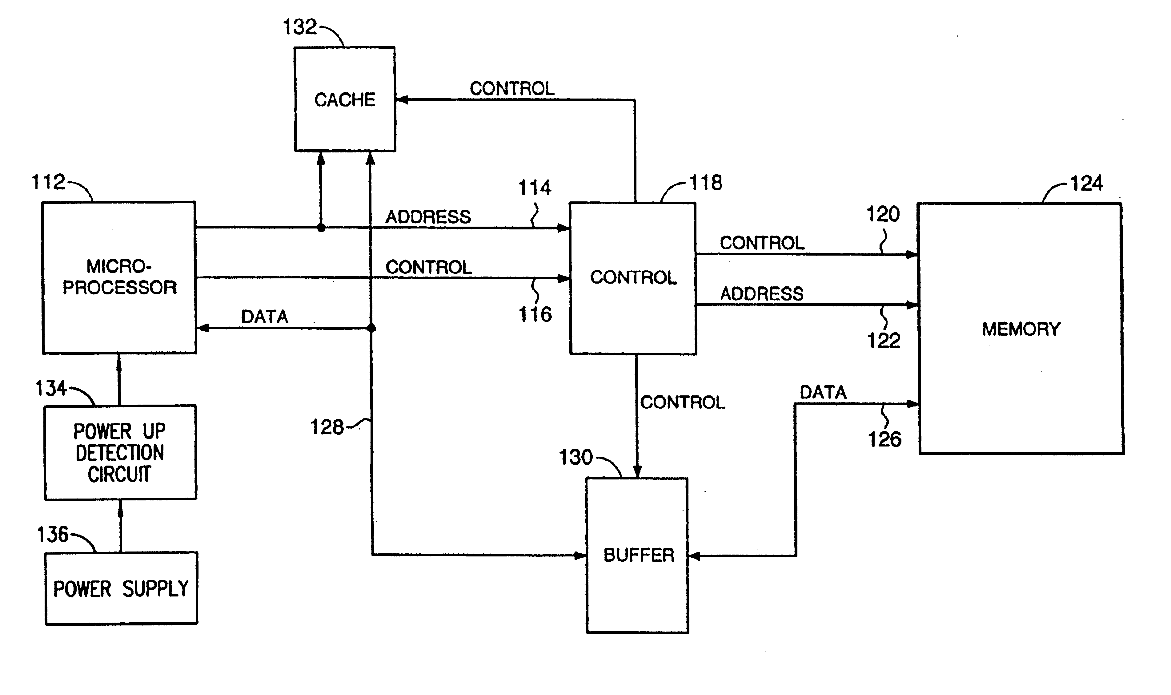
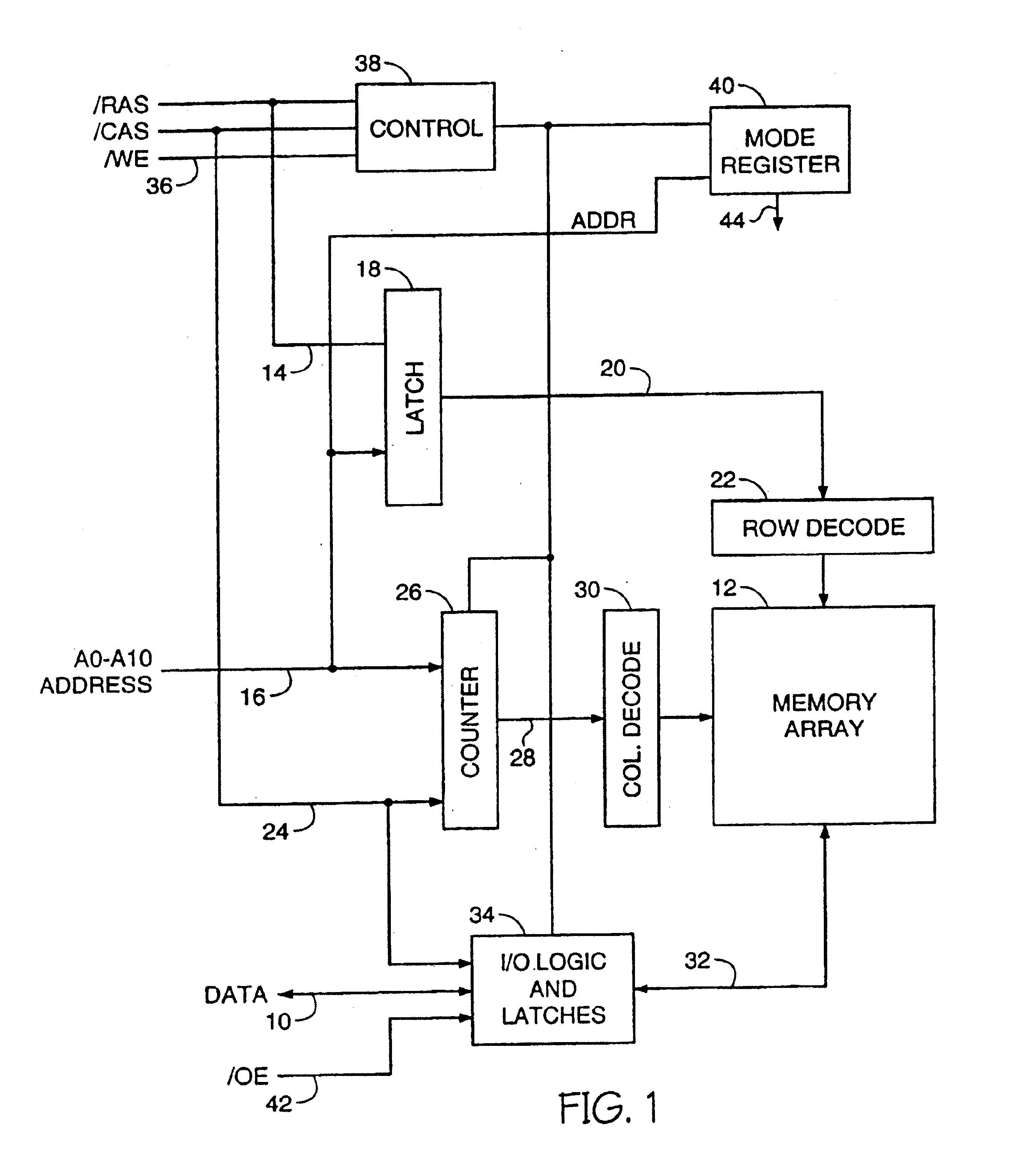
[0024]FIG. 1 is a schematic representation of a sixteen megabit device designed in accordance with the present invention. The device is organized as a 2 Meg×8 burst EDO DRAM having an eight bit data input / output path 10 providing data storage for 2,097,152 bytes of information in the memory array 12. The device of FIG. 1 has an industry standard pinout for eight bit wide EDO DRAMs. An active-low row address strobe ( / RAS) signal 14 is used to latch a first portion of a multiplexed memory address, from address inputs A0 through A1016, in latch 18. The latched row address 20 is decoded in row decoder 22. The decoded row address is used to select a row of the memory array 12. A column address strobe ( / CAS) signal 24 is used to latch a second portion of a memory address from address inputs 16 into column address counter 26. The latched column address 28 is decoded in column address decoder 30. The decoded column address is used to select a column of the memory array 12.

[0025]In a burst r...


PUM


Abstract

A system is capable of receiving Fast Page mode, Extended Data Out mode, Burst Extended Data Out mode, or a combination of these memory devices. A method of determining the type of memory present allows the system to adjust internal memory access signals in accordance with the type of memory installed. The system may be shipped with a first type of memory, and then upgraded to a second type of memory by the user to improve overall system performance. A first bank of memory may be of a first type, and a second bank may be of another type. The user may make cost versus performance decisions when upgrading memory types or capacities.

Description

[0001]This application is a continuation of U.S. Ser. No. 08 / 457,650 filed Jun. 1, 1995, now U.S. Pat. No. 6,804,760, [which is a continuation-in-part of U.S. Ser. No. 08 / 386,894 filed Feb. 10, 1995, now U.S. Pat. No. 5,610,864, which is a continuation-in-part of U.S. Ser. No. 08 / 370,761 filed Dec. 23, 1994, now U.S. Patent No. 5,526,320.]FIELD OF THE INVENTION[0002]This invention relates to system architectures adapted to receive multiple types of memory devices and methods of determining the type of memory present.BACKGROUND OF THE INVENTION[0003]Dynamic Random Access Memory devices (DRAMs) are among the highest volume and most complex integrated circuits manufactured today. Except for their high volume production, the state of the art manufacturing requirements of these devices would cause them to be exorbitantly priced. Yet, due to efficiencies associated with high volume production, the price per bit of these memory devices is continually declining. The low cost of memory has f...

Claims


Application Information

Patent Timeline
IPC IPC(8): G06F12/00G11C7/00G06F12/06G11C7/10G11C11/401G11C11/407
CPCG06F12/0638G11C7/1021G11C7/1024G11C11/407G11C7/1045G11C7/1078G11C7/109G11C7/1096G11C7/1039G06F2212/2022
Inventor WILIAMS, BRETT L.
Owner ROUND ROCK RES LLC
Why Eureka
Try Eureka