[0043]According to another preferred embodiment a PEALD reactor (see FIG. 5) that is suitable for in situ
plasma discharge is used. In PEALD, one deposition cycle typically comprises four basic process steps. First, a metal precursor is pulsed from a first source 508 through a first source conduit 510 and through a showerhead 526 into a reaction space 520 of a reactor 500 provided with a substrate 524. Second, excess metal precursor and gaseous reaction byproducts are purged from the reaction space 520 to the exhaust line 504 of the reactor 500. Third, a non-metal source chemical is pulsed from a
second source 512 through a
second source conduit 514 and through the showerhead 526 into the reaction space 520. Simultaneously,
plasma power is switched on to provide an activated form of the non-metal source chemical preferably inside the showerhead 526 space. The non-metal source chemical, in its inactive form may be the same as gas the purging gas (e.g.
nitrogen). The activated form of the non-metal source chemical is capable of forming a
solid compound during a
surface reaction with metal precursor that is chemisorbed on the surface of the substrate 524. Finally, excess source chemicals and the gaseous byproducts formed in the surface reactions are purged into the exhaust line 504 of the reactor 500. The last purging step can be very short, i.e. less than 0.1 seconds, because switching the
plasma power off terminates the generation of active non-metal species. However, in the embodiment of this invention, any byproducts of the surface reactions are purged away in order to achieve the desired effect of the invention.
[0044]According to one more embodiment of the present invention an RA-ALD reactor shown in FIG. 6 is used. RA-ALD implements
remote plasma discharge principles. One deposition cycle comprises at least of the above-mentioned sequence of two pulsing and two purging steps. The first pulsing step comprises providing to the reaction space 620 metal source chemical molecules that are vaporized in the first source 608 and guided preferably with inactive carrier gas through the first source conduit 610 and through the showerhead 626. The excess metal source chemical vapor and reaction byproducts are purged away from the reaction space 620 of the reactor 600.
[0045]The vapor pulse of the second pulsing step comprises activated non-metal species. When
remote plasma discharge is applied, the activated form of the non-metal source chemical is created in the
remote plasma source 612 area and the activated species are introduced to the reaction space 620 through the remote plasma source conduit 614 and through the showerhead 626. The activated species react with the chemisorbed metal source
chemical species on the
substrate surface, thus forming
solid film up to one atomic or molecular layer per depositing cycle. The pulsing sequence ends with the second purge that removes excess activated species and reaction byproducts from the reaction space 620 to the exhaust conduit 604 and the
vacuum pump 602. Gases are discharged from the
vacuum pump 602 to the
vacuum pump exhaust 606 and treated properly to remove harmful components from the
exhaust gas stream. The pulsing sequence is repeated until a thin film of desired thickness is deposited on the substrate 624. The order of the precursor pulses can also be changed so that the activated species are pulsed prior to the metal source chemical vapor pulses. In the preferred embodiments, the precursor pulses are always separated from each other with the purging steps evacuating the reaction space from the excess of the precursor species and gaseous reaction byproducts.
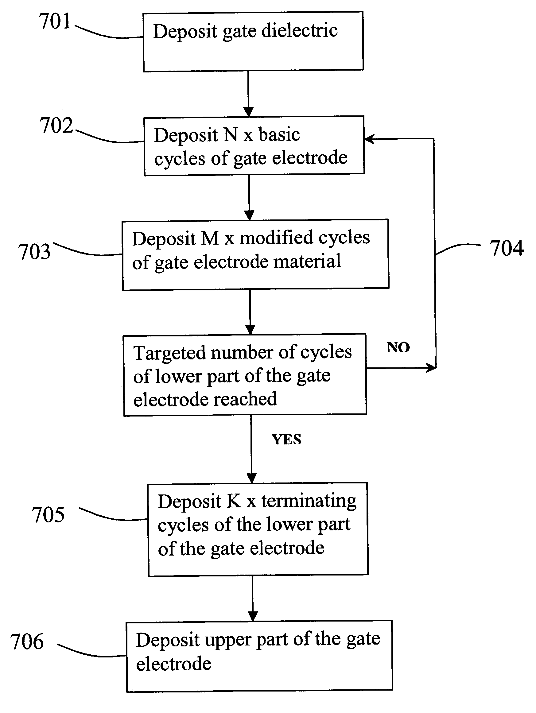
[0046]The overall work function of the gate electrode deposited according to the preferred embodiments is tuned to a desired value by modifying the composition of the gate
electrode material, particularly the lower part of a composite gate electrode. The composition is changed, for example, by selecting a suitable scheme of differentiated pulsing cycles for the deposition of the lower gate electrode layer in ALD type process.
[0047]
Electronegativity depends on the composition of a material and affects the work function. In order to utilize the relation between the composition of the gate
electrode material and the work function, theoretical tools are applied to find suitable compounds.
Experimental work further helps to fine-tune the composition of the material and to reach the target work function. One method for estimating the
electronegativity of a compound utilizes electronegativity scales.
[0048]Pauling's scale is perhaps the most famous electronegativity scale. In context of the present invention, the overall electronegativity of a compound thin film can be understood via the electronegativity
equalization principle. The overall electronegativity refers to the electronegativity of the compound and it is calculated by electronegativity
equalization principle. This method for evaluating the overall electronegativity is based on Sanderson's principle of electronegativity
equalization and it is presented in Eq. 1.

