Field-effect type semiconductor device for power amplifier

a power amplifier and field-effect technology, applied in semiconductor devices, semiconductor devices, amplifiers with semiconductor devices/discharge tubes, etc., can solve the problems of reducing the mobility of carriers, reducing the efficiency of wafers, and reducing the cost of wafers. the effect of reducing leakage current, improving carrier mobility, and improving transconductan

Inactive Publication Date: 2006-05-16
TESSERA ADVANCED TECH
View PDF15 Cites 9 Cited by
  • Summary
  • Abstract
  • Description
  • Claims
  • Application Information

AI Technical Summary

Benefits of technology

[0011]On the other hand, when the silicon semiconductor (Si) disclosed in reference 3 is applied, the wafer unit price is cheaper than that in the case of the compound semiconductor. In addition, the existing Si process technology can be applied to advantage.
[0012]However, because of a limited property of matter of Si, the efficiency can only be increased limitedly. More specifically, for promotion of the performance of the Si-MOSFET, decreasing the gate oxide film thickness and shortening the channel length have hitherto been effective but such scaling as above has not at last be connected directly to the performance promotion. In other words, the more the scaling advances, the more the effective mobility in the channel decreases. This is because a strong electric field is applied to an interface to the gate oxide film and consequently, the carrier density increases and scattering of carriers are accelerated. As a result, carriers are pressed against the interface to the gate oxide film, and scattering of carriers increases to decrease the carrier mobility. Accordingly, the channel conductance having control of the performance of the Si-MOSFET can be decreased only limitedly.
[0019]Another object of the invention is to provide a technique of reducing size and weight of a high-frequency power amplifier.
[0022]With the above construction, the region containing a large quantity of crystal defects (dislocation) caused by bonding different lattice sizes is so conditioned as to be confined in the first SiGe layer of relatively high impurity concentration. The depletion layer extending from the drain region sufficiently expands until the first SiGe layer of relatively low impurity concentration and when it comes to the first SiGe layer of high impurity concentration, its expansion is suppressed. Therefore, the depletion layer will not expand to the region containing the large quantity of crystal defects (dislocation). Accordingly, the depletion layer expansion limited to the second SiGe layer (low-concentration layer) can assure the drain breakdown voltage and the suppression of the depletion layer expansion at the first SiGe layer (high-concentration layer) can reduce the leakage current. In addition, the strained Si having tensile strain is formed on the surface of the second SiGe layer and this strained Si is used as the channel region, with the result that the band structure is changed by the strain and the carrier mobility can be improved by about 70% as compared to that with unstrained Si. Accordingly, the transconductance can be improved and a power semiconductor device of high performance can be provided.

Problems solved by technology

The application of the compound semiconductor has raised a problem of an expensive unit price of wafer.
However, because of a limited property of matter of Si, the efficiency can only be increased limitedly.
As a result, carriers are pressed against the interface to the gate oxide film, and scattering of carriers increases to decrease the carrier mobility.
In order to improve the effective mobility, control of impurity profile responsible for relaxing the electric field in the channel, for example, is conceivable but owing to the limited threshold voltage and a limited decrease in the power supply voltage (at present, 3.5V of lithium battery), especially, in the case of a high-frequency power MOSFET, the expedient as above has failed to play an eminent role in performance improvement.

Method used


Image

  • Field-effect type semiconductor device for power amplifier
  • Field-effect type semiconductor device for power amplifier
  • Field-effect type semiconductor device for power amplifier

Examples


embodiment 1

(Embodiment 1)

[0036]In the present embodiment, an N-channel field-effect type semiconductor device is exemplified in which a channel is formed in a Si layer formed on a SiGe layer.

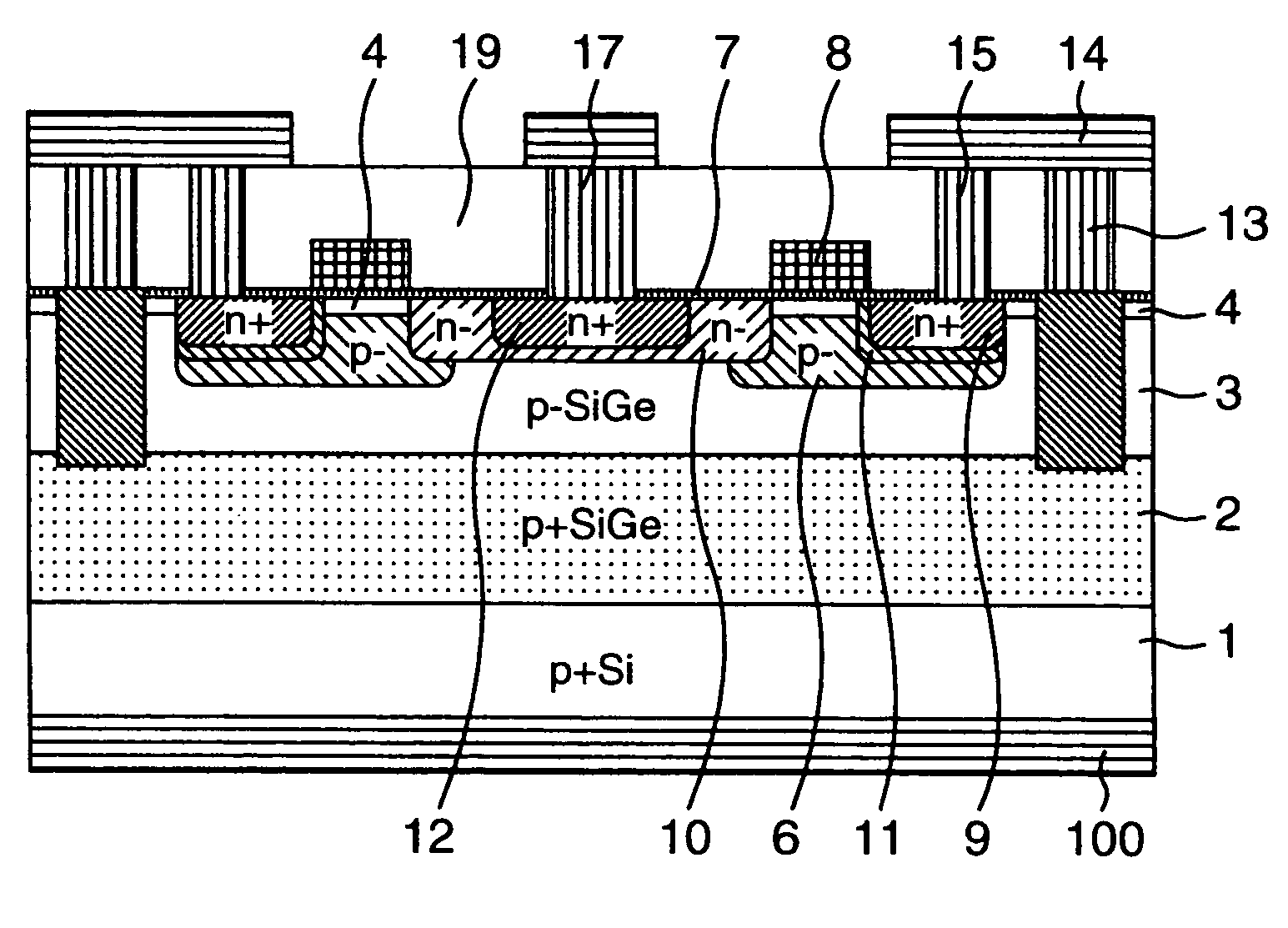
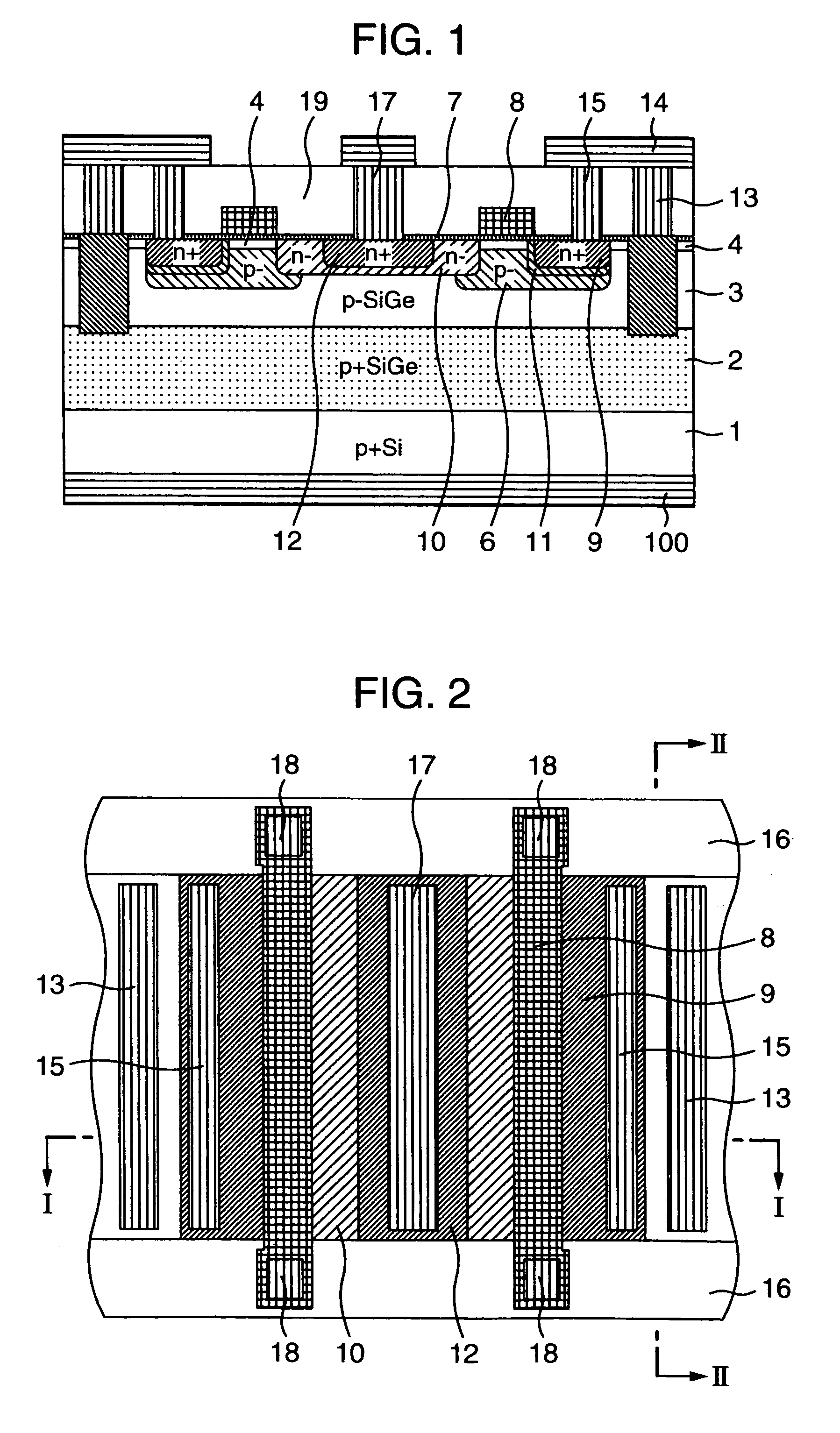
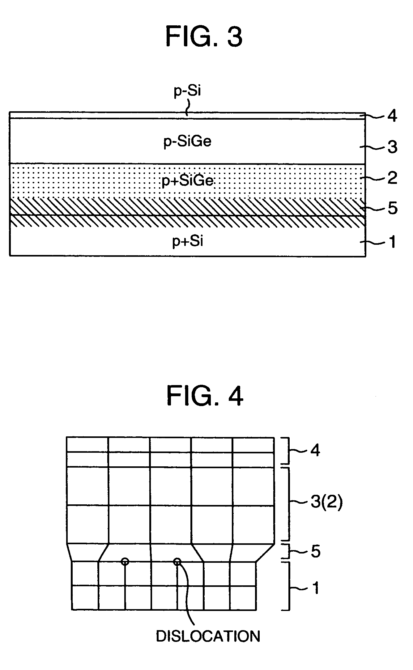
[0037]FIG. 1 is a longitudinal sectional view of essential part of an N-channel field-effect type semiconductor device according to the present embodiment and FIG. 2 is a plan view of the N-channel field-effect type semiconductor device. Specifically, the FIG. 1 sectional view shows a section taken on line I—I in FIG. 2. Prior to giving a description with reference to FIGS. 1 and 2, a semiconductor multi-layer structure used in the fabrication of the field-effect semiconductor device of embodiment 1 will be described by making reference to FIGS. 3 and 4.

[0038]As shown in FIG. 3, in the semiconductor multi-layer structure used in the fabrication of the field-effect type semiconductor device according to embodiment 1, a P-type low-resistance first SiGe layer 2, a P-type high-resistance second SiGe layer 3 an...

embodiment 2

(Embodiment 2)

[0058]In the present embodiment, there is exemplified a P-channel field-effect type semiconductor device in which a channel is formed in a Si layer formed on a SiGe layer. The fabrication process extremely resembles that in the case of embodiment 1 and only different points will be described.

[0059]The semiconductor multi-layer structure shown in FIG. 3 is structurally altered in the present embodiment to have an N-type low resistance Si substrate 1, an N-type low resistance first SiGe layer 2, an N-type high resistance second SiGe layer 3 and an N-type high resistance Si layer 4. As a doping gas, PH3 is used in place of the B2H6 and the impurity concentration is similar to that in embodiment 1.

[0060]The well region 6 and punch-through stopper 11 are of N-type and for them, P is implanted in place of B. Each of the source region 9, drain region 12 and drain offset region 10 is of P-type and for its formation, B or BF2is implanted. The ion implantation depth and implanta...

embodiment 3

(Embodiment 3)

[0062]In the present embodiment, a P-channel field-effect type semiconductor device will be exemplified in which a channel is formed near an interface to Si layer 4 inside the second SiGe layer 3. The fabrication process extremely resembles that in embodiment 2 and only different points will be described.

[0063]When, in the foregoing semiconductor multi-layer structure, the thickness of Si layer 4 is set to 15 nm, the thickness of the Si layer 4 in a channel region of a completed field-effect transistor is less than 5 nm and as a result, the channel is not formed in the Si layer 4 but is formed near an interface to Si layer 4 inside the second SiGe layer 3.

[0064]In the present transistor the hole mobility in the second SiGe layer 3 is 2.1 times increased to advantage as compared to that of the ordinary Si field-effect transistor and the transconductance is improved by 90% as compared to the conventional transistor to 75% improve the power added efficiency of power ampli...


PUM


Abstract

In a semiconductor multi-layer structure in which a first SiGe layer having a first conductivity-type and high impurity concentration, a second SiGe layer having the first conductivity-type and a low impurity concentration and a Si layer having a low impurity concentration are formed one on another in this order on a Si substrate of the first conductivity-type, a channel is formed in a part of the Si layer and a source electrode passes through the second SiGe layer of low impurity concentration to electrically contact the first SiGe layer of high impurity concentration or the substrate.

Description

[0001]This is a continuation application of U.S. Ser. No. 10 / 259,396, filed Sep. 30, 2002 now U.S. Pat No. 6,815,707.BACKGROUND OF THE INVENTION[0002]The present invention relates to field-effect type semiconductor devices and more particularly to a technique effectively applicable to a field-effect type semiconductor device for high-frequency power amplification of not less than 800 MHz used in a mobile communication unit.[0003]With widespread use of a mobile communication terminal in recent years, a power amplifier for portable terminal of lower power consumption and higher efficiency has been demanded increasingly. For a power amplification device directed to this utilization, a transistor (HBT) using a compound semiconductor (HBT) or an insulated gate field-effect transistor (Si-MOSFET) using a silicon semiconductor (Si) has been used.[0004]A power amplifier using the compound semiconductor is described in, for example, IEEE Journal of Solid-state Circuits, Volume:35 Issue: 8, p...

Claims


Application Information

Patent Timeline
Patent Type & Authority Patents(United States)
IPC IPC(8): H01L21/8238H01L21/336H01L21/8234H01L27/088H01L27/092H01L29/10H01L29/165H01L29/78H03F3/60
CPCH01L29/165H01L29/7835H03F3/601H01L29/66659H01L29/1045H01L29/1087Y10S438/933
Inventor SUGII, NOBUYUKIMORIKAWA, MASATOSHIYOSHIDA, ISAOWASHIO, KATSUYOSHI
Owner TESSERA ADVANCED TECH
Why Eureka
Try Eureka