Calibration standard for critical dimension verification of sub-tenth micron integrated circuit technology

a technology of integrated circuit technology and critical dimension verification, which is applied in the field of testing and diagnostic, can solve the problems of poor dimensional uniformity, edge roughness, and compromise of desirability of calibration standards, and achieve low width roughness, low edge roughness, and low charging.

Inactive Publication Date: 2006-05-23
TAIWAN SEMICON MFG CO LTD
View PDF13 Cites 8 Cited by
  • Summary
  • Abstract
  • Description
  • Claims
  • Application Information

AI Technical Summary

Benefits of technology

[0012]It is a another object of this invention to provide a method for forming precision trenches in a metal layer with low width roughness, low edge roughness, and with reduced charging.

Problems solved by technology

Unfortunately, polysilicon lines patterned by these conventional photolithographic and etching processes, which are the essentially the same as those used to manufacture the IC product, suffer from a number of problems which compromise their desirability as calibration standards.
These problems include edge roughness and poor dimensional uniformity.
In addition, because the lines are of polysilicon, they tend to become charged during the SEM measurement resulting in serious image distortion.
Progress was relatively slow with regard to patterning with a focused ion beam (FIB) slow because, like electron beam patterning, it took a relatively long time to pattern photoresist on a wafer by scanning a single beam.
Furthermore, FIB systems could not bring about high ion currents at small spot size.
Nevertheless, full wafer patterning of today's large wafers with a single FIB is still not practical.

Method used


Image

  • Calibration standard for critical dimension verification of sub-tenth micron integrated circuit technology
  • Calibration standard for critical dimension verification of sub-tenth micron integrated circuit technology
  • Calibration standard for critical dimension verification of sub-tenth micron integrated circuit technology

Examples


Embodiment Construction

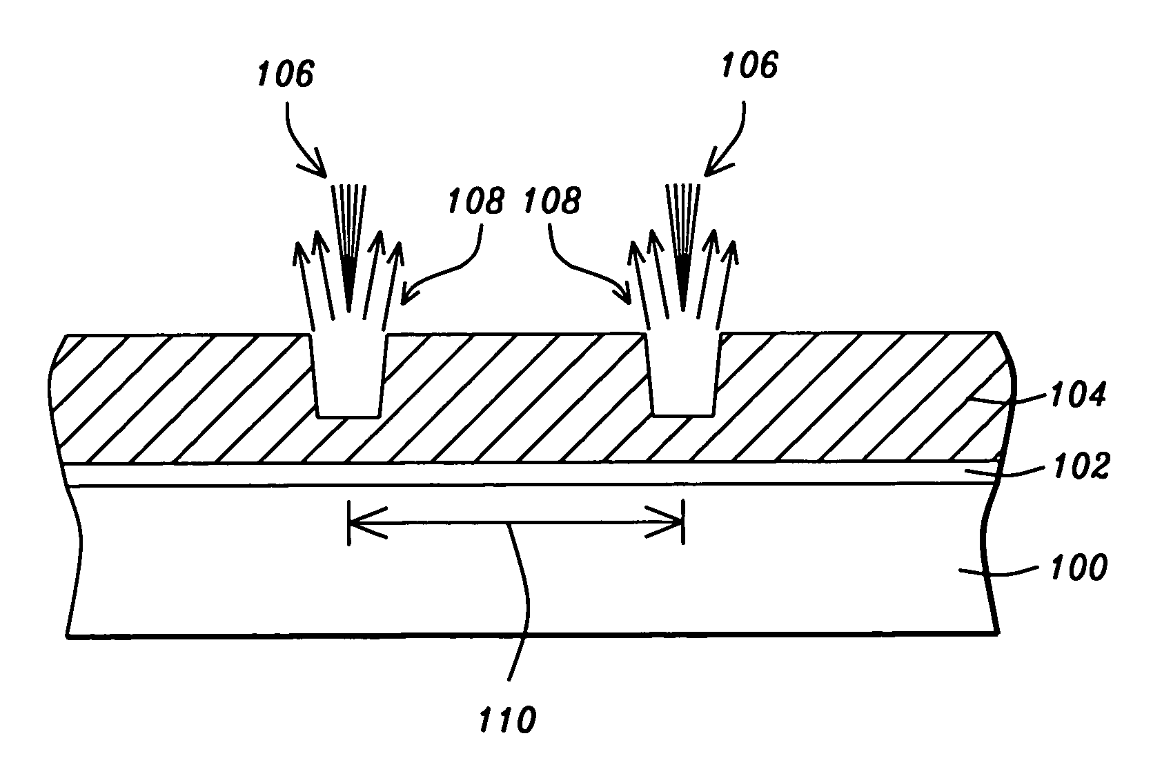
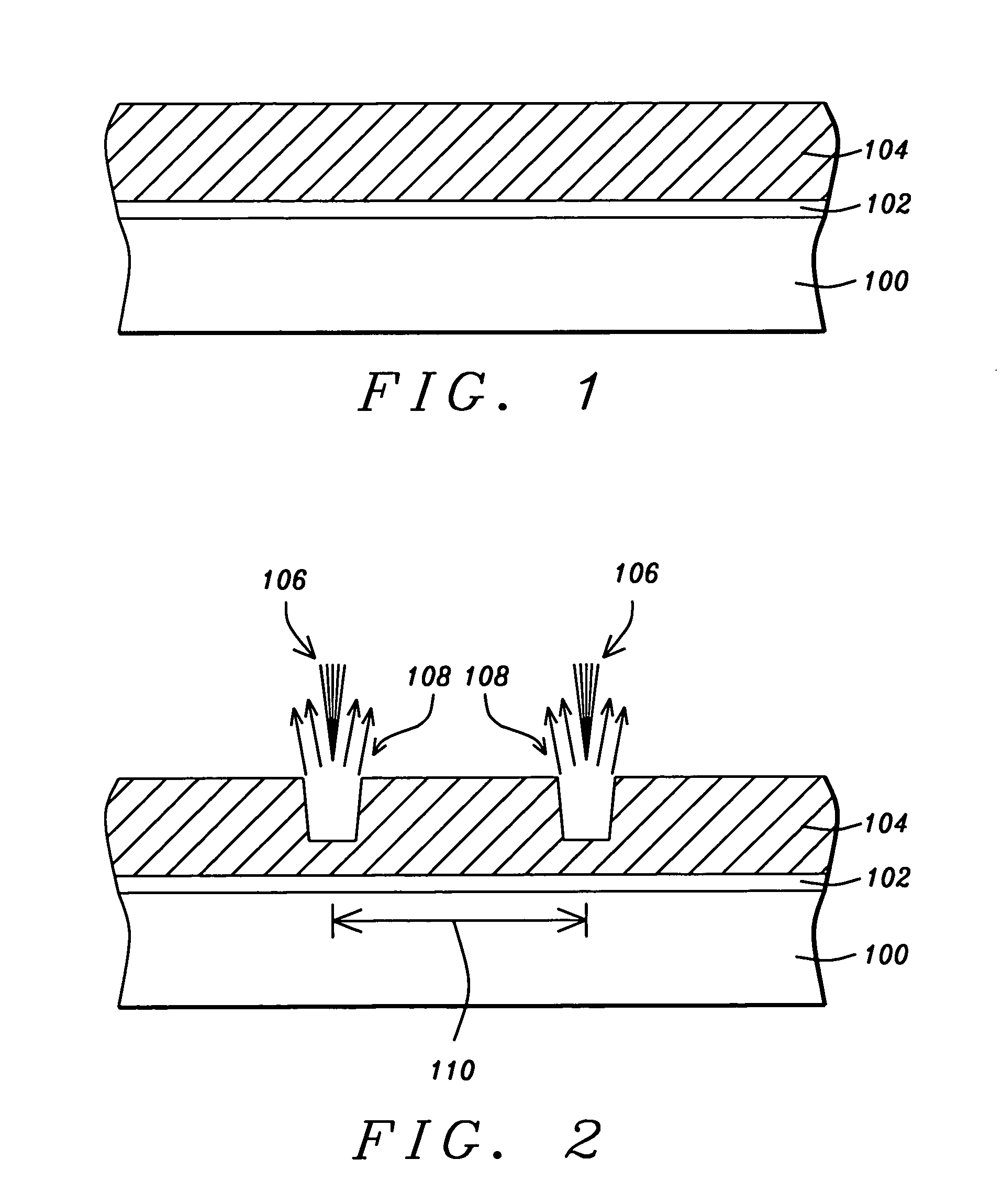
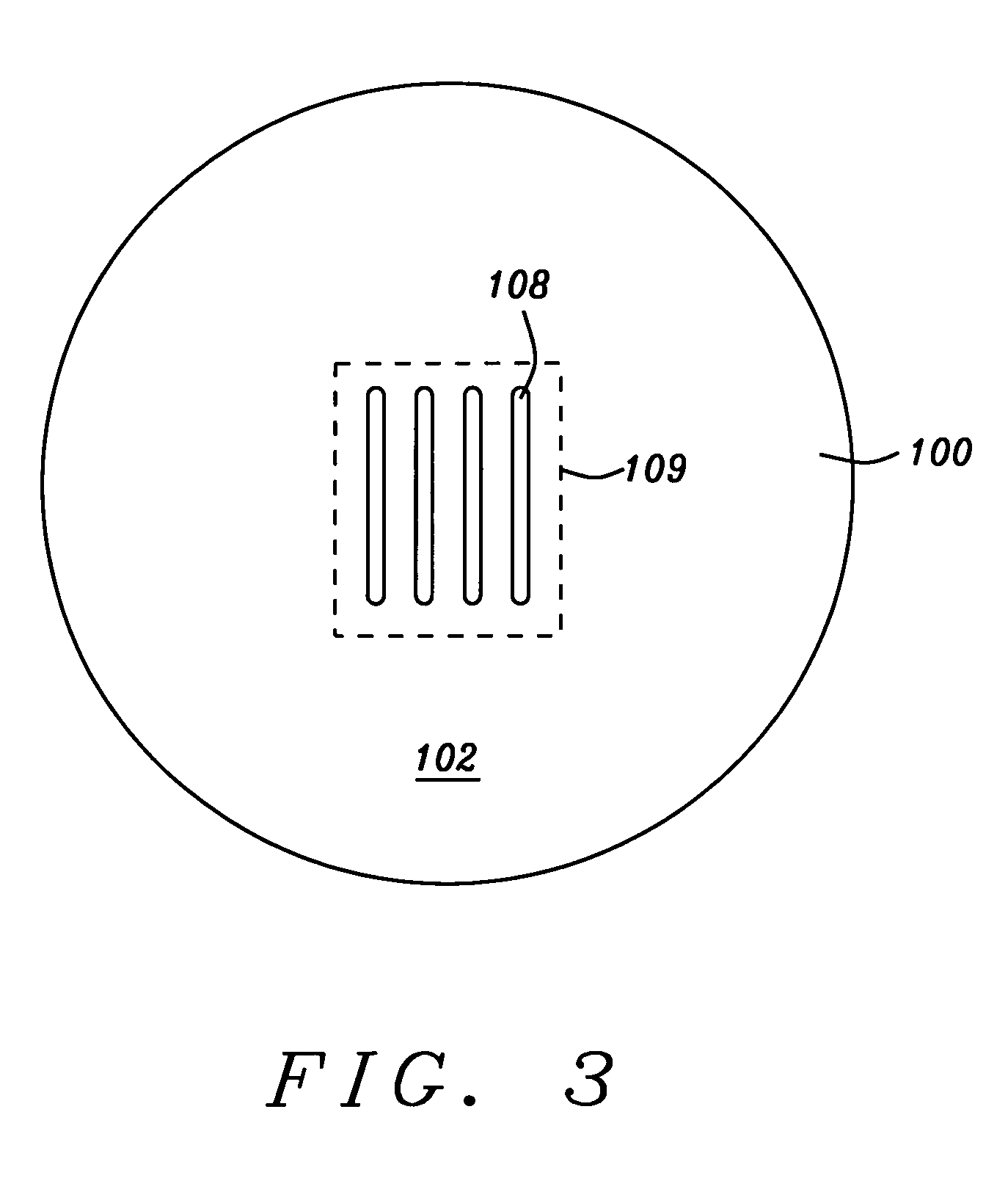
[0022]In an embodiment of this invention an SEM calibration pattern will be formed on a silicon wafer. The calibration pattern consists of a set of parallel trenches dug into a metal layer using a focused ion beam. The widths of the trenches will be of the order of 50 nm. The widths of the metal lines which separate the trenches is arbitrary and may typically exceed 500 nm. The widths of the trenches and metal lines are verified by measurement in a laboratory calibrated SEM. After calibration, the wafer is used in a manufacturing environment as reference for calibration of SEMs, used to monitor critical dimensions of integrated circuit product flowing through a process line. The wafer may also used to verify and monitor the stability of the SEMs.

[0023]Referring to FIG. 1, a silicon wafer 100 is provided. A thin silicon oxide pad layer 102, between about 50 and 200 nm. thick is thermally grown on the wafer 100 by conventional thermal oxidation. The pad oxide layer 102 serves as a str...


PUM


Abstract

A critical dimension control wafer for calibrating process control scanning electron microscopes is described. The test wafer provides one or more test structures each consisting of an array of parallel trenches precision micro-machined in a metal plate. The trenches are formed, preferably in an aluminum / copper alloy plate, using focused ion beam milling. The micro-machined trenches have lower width roughness and lower edge roughness compared to similar patterns form in polysilicon by conventional photo lithographic methods. In addition, electron charging in the scanning electron microscope, which produces distorted images, is essentially eliminated. The dimensions of the trenches and the metal lines between them have dimensions comparable to those of polysilicon lines used in sub-tenth micron integrated circuit process technology control wafer. The control wafers are calibrated using a calibrated laboratory grade scanning electron microscope. Once calibrated, the control wafers may be stock-piled for subsequent routine use as a high precision dimensional reference, in particular for calibrating and monitoring the stability of process line scanning electron microscopes.

Description

BACKGROUND OF THE INVENTION[0001](1) Field of the Invention[0002]This invention relates to testing and diagnostics of line processes used for the manufacture of integrated circuit devices and more particularly to critical dimensional measurement of sub-tenth micron pattern features during wafer processing.[0003](2) Description of Prior Art[0004]The manufacture of large scale integrated circuits in a mass production facility involves hundreds of discrete processing steps beginning with the introduction of blank semiconductor wafers at one end and recovering the completed chips at the other. The manufacturing process is usually conceived as consisting of the segment wherein the semiconductor devices are formed within the silicon surface (front-end-of-line) and the portion which includes the formation of the various layers of interconnection metallurgy above the silicon surface (back-end-of-line). Most of these processing steps involve depositing layers of material, patterning them by ...

Claims


Application Information

Patent Timeline
Patent Type & Authority Patents(United States)
IPC IPC(8): H01L21/76H01L23/58H01L21/302
CPCH01L22/34G01N2223/303H01J2237/2826
Inventor LU, YU-HUIWU, TIEN-CHI
Owner TAIWAN SEMICON MFG CO LTD
Why Eureka
Try Eureka