

Vertical gain cell and array for a dynamic random access memory and method for forming the same
a dynamic random access and gain cell technology, applied in the field of semiconductor memory devices, can solve the problems of destructive and transient read operation of the device, dwindling surface space on the silicon chip/die that is allocated to each transistor, and difficulty in maintaining sufficient cell capacitance, etc., to achieve increased cell density, increased capacitance, and increased data retention time
- Summary
- Abstract
- Description
- Claims
- Application Information
AI Technical Summary
Benefits of technology
Problems solved by technology
Method used
Image

Examples
Embodiment Construction
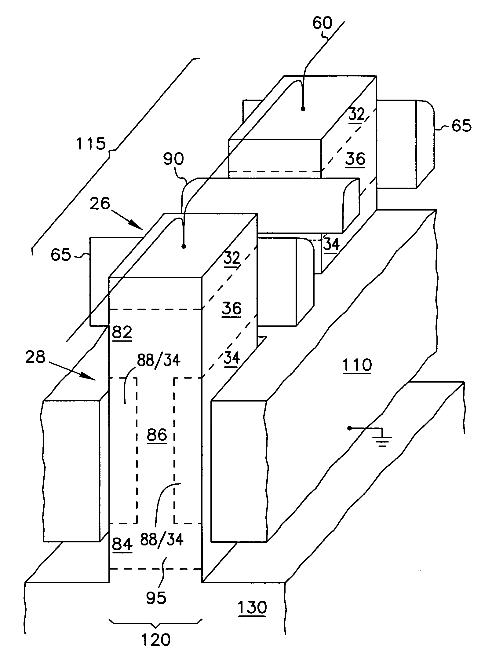
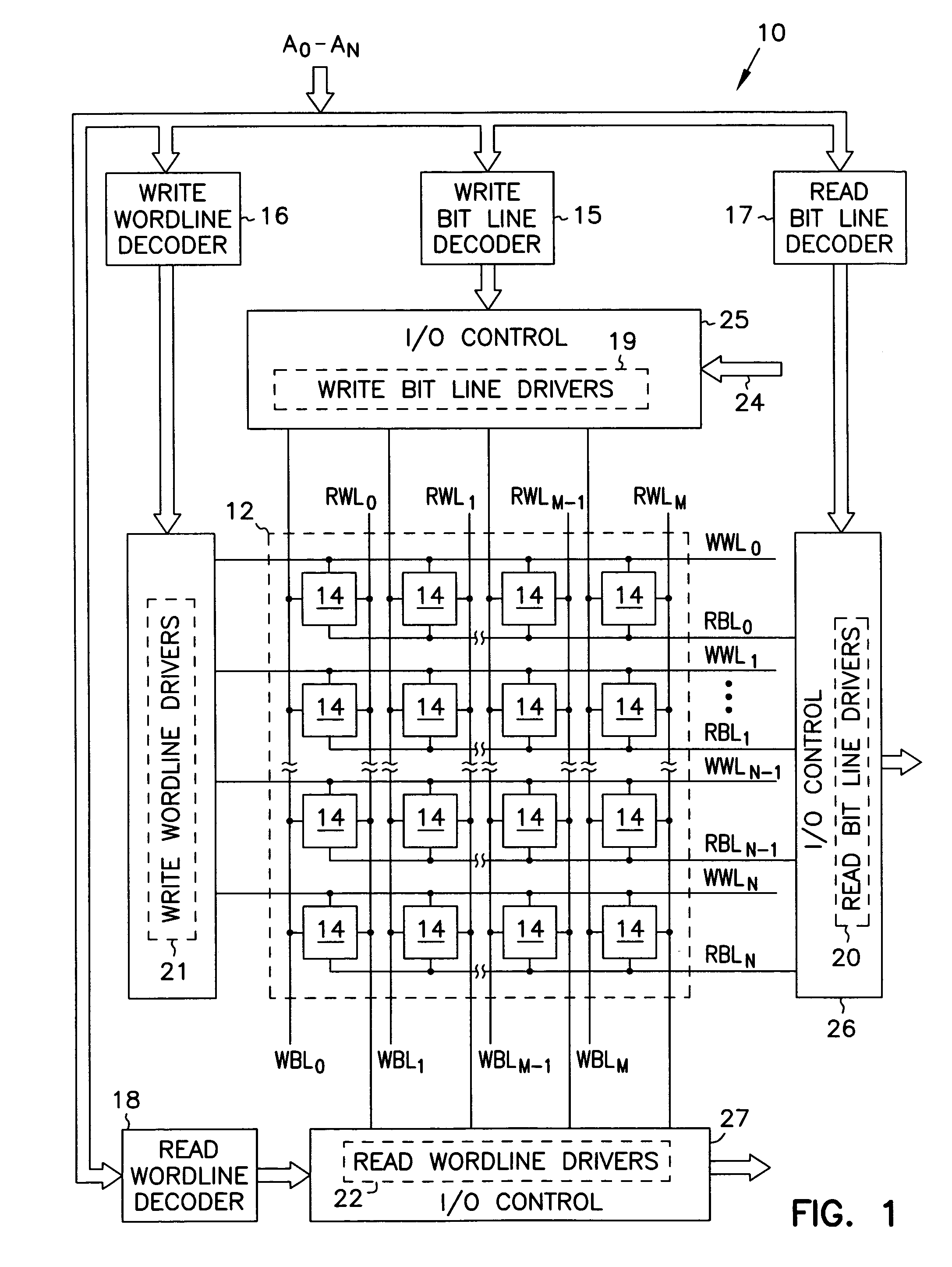
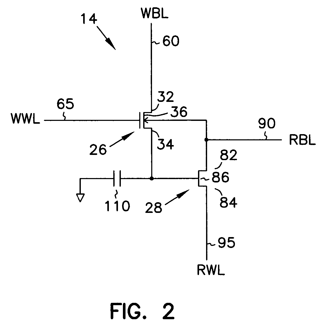
[0023]In the following detailed description of the invention, reference is made to the accompanying drawings which form a part hereof, and in which is shown, by way of illustration, specific embodiments in which the invention may be practiced. These embodiments are described in sufficient detail to enable those skilled in the art to practice the invention. Other embodiments may be utilized and structural, logical, and electrical changes may be made without departing from the scope of the present invention. The terms wafer and substrate used in the following description include any structure having an exposed surface with which to form the integrated circuit (IC) structure of the invention. The term substrate is understood to include semiconductor wafers. The term substrate is also used to refer to semiconductor structures during processing, and may include other layers that have been fabricated thereupon. Both wafer and substrate include doped and undoped semiconductors, epitaxial s...
PUM
 Abstract
Description
Claims
Application Information