Semiconductor integrated circuit device and semiconductor integrated circuit

a technology of integrated circuit and semiconductor, which is applied in logic circuit coupling/interface arrangement, baseband system details, pulse manipulation, etc., can solve the problems of unavoidable expansion of chip size, inability to avoid significant increase of chip size, and another conventional problem, so as to prevent input data signals, prevent signal amplitude reduction, and prevent duty distortion

Active Publication Date: 2006-05-30
ABLIC INC
View PDF10 Cites 14 Cited by
  • Summary
  • Abstract
  • Description
  • Claims
  • Application Information

AI Technical Summary

Benefits of technology

[0021]According to the method described above, both of low and high frequency components of input signals are amplified, so that input data signals are prevented from amplitude variation and signal jitter increasing that occur due to the dependency on the array of transmitted data even when the data signals are transferred faster. Data can thus be transferred accurately to the subject internal circuit. And, while a capacitor to be connected to an input terminal and a pair of second differential input transistors for amplifying the high frequency components of input signals are required for the input circuit, the capacitor can be formed in an area smaller than that of an inductor in the semiconductor integrated circuit, so that the chip is not expanded so much in size to latch and transfer fast data signals to the internal circuit free from distortion of their waveforms.
[0022]Furthermore, because the input circuit that latches a clock pulse signal inputted from external to supply it to an internal circuit can amplify both low and high frequency components of the input signal, the signal is prevented from amplitude reduction even when the clock frequency rises. The clock signal can thus be prevented from duty distortion, thereby the circuit that latches data signals synchron

Problems solved by technology

It is thus impossible to avoid a significant increase of the chip size.
This is still another conventional problem.
And, because the number of elemen

Method used


Image

  • Semiconductor integrated circuit device and semiconductor integrated circuit
  • Semiconductor integrated circuit device and semiconductor integrated circuit
  • Semiconductor integrated circuit device and semiconductor integrated circuit

Examples


first embodiment

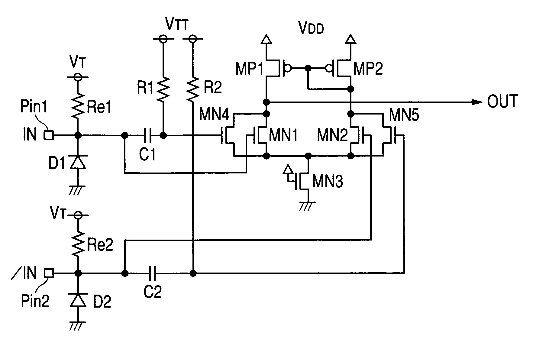
[0051]FIG. 1 shows a differential input circuit (hereinafter, to be referred to just as the input circuit) in the present invention.

[0052]In FIG. 1, Pin 1 and Pin 2 denote input terminals to which differential input signals IN and / IN are inputted from external. In a semiconductor integrated circuit, these input terminals are generally formed as electrodes referred to as bonding pads connected to one end of bonding wire respectively or pads connected to the package side electrodes through a solder ball or the like respectively.

[0053]The input circuit in this first embodiment is configured by a pair of N-channel differential input MOSFETs MN1 and MN2, each having a source terminal connected to that of the other to form a common source and a gate terminal connected to one of the pair of input terminals Pin1 and Pin2; a pair of N-channel differential input MOSFETs MN4 and MN5, each having a source terminal connected to that of its corresponding N-channel differential input MOSFET MN1 / M...

second embodiment

[0078]FIG. 7 shows an input circuit in the present invention.

[0079]The input circuit in this second embodiment is modified from that in the first embodiment so that N-channel MOSFETs are replaced with P-channel MOSFETs MP1 to MP5 used as both differential input and current generators and P-channel load MOSFETs are replaced with N-channel load MOSFETs MN1 and MN2. The input circuit in this second embodiment is characterized in that the center potential to be supplied to the internal circuit can be set lower than that of the input circuit in the first embodiment.

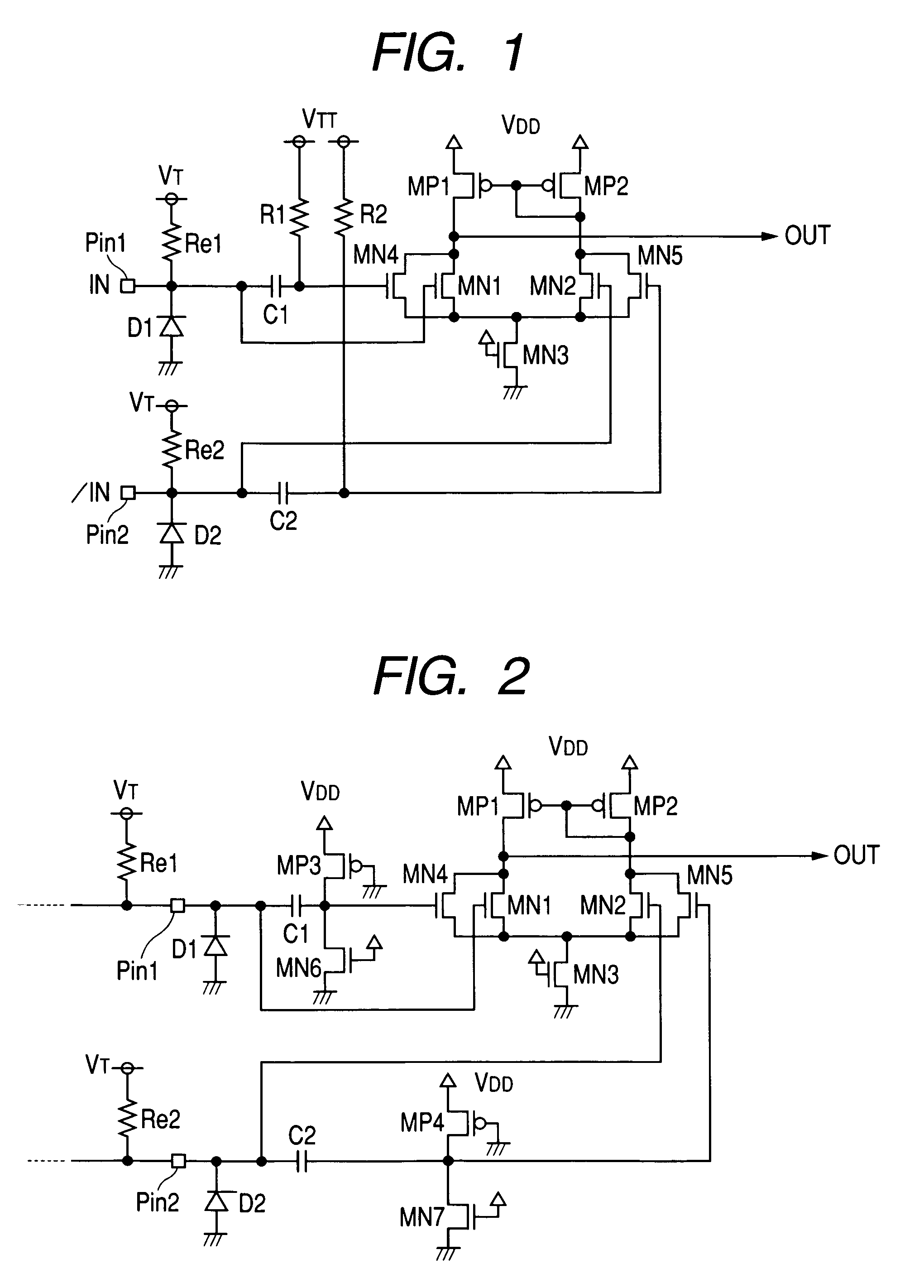
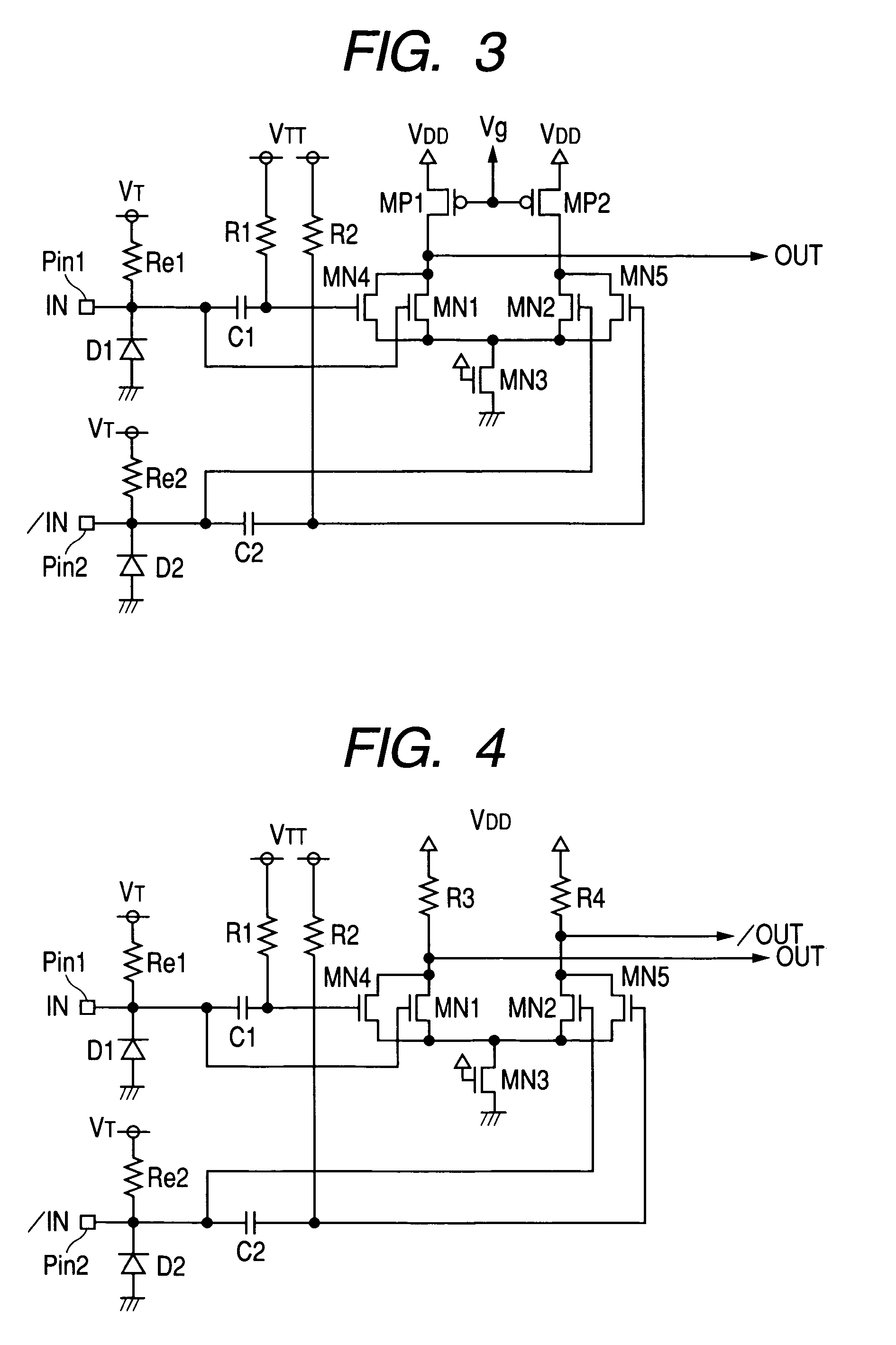
[0080]FIG. 8 shows a variation of the input circuit in this second embodiment. The variation is equivalent to that of the first embodiment, shown in FIG. 3. FIG. 9 shows another variation of the input circuit in this second embodiment. The variation is equivalent to that of the first embodiment, shown in FIG. 4. Although not shown in any drawing, other variations are also possible. For example, the resistors R1 and R2 in the i...

third embodiment

[0081]FIG. 10 shows an input circuit in the present invention.

[0082]The input circuit in this third embodiment is configured so as to receive the differential input signals IN and / IN at the P-channel differential input MOSFETs MP1, MP2, MP4, and MP5, as well as at the N-channel differential input MOSFETs MN1, MN2, MN4, and MN5. The drains of the P-channel and N-channel differential input MOSFETs MP1, MP2, MP4, and MP5 are connected to a ground point through the load elements R13 and R14 respectively while the drains of the N-channel differential input MOSFETs MN1, MN2, MN4, and MN5 are connected to the supply voltage terminal VDD through the load elements R11 and R12 respectively.

[0083]MOSFETs MP8 and MN8 used to set the center potential of each output signal are connected to each other serially between the load elements R11 and R13 while MOSFETs MP9 and MN9 used to set the center potential of each output signal are connected to each other serially between the load elements R12 and...


PUM


Abstract

Disclosed herewith is a semiconductor integrated circuit provided with a differential input circuit that can transmit data signals fast to an internal circuit free from distortion of their waveforms without increasing the subject chip in size. The differential input circuit is provided with a pair of first differential input transistors used to amplify mainly the low frequency components of those input signals and having gate terminals connected to a pair of input terminals that receive inputs of differential signals respectively, as well as a pair of second differential input transistors used mainly to amplify high frequency components of those input signals and having control terminals connected to a pair of input terminals that receive inputs of differential signals respectively through capacitance elements. The pairs of first and second differential transistors are connected to each other through a differential connection point (common source).

Description

PRIORITY CLAIM[0001]This application claims priority under 35 USC §119 to Japanese patent application P2003-001825 filed Jan. 8, 2003, the entire disclosure of which is hereby incorporated herein by reference.FIELD OF THE INVENTION[0002]The present invention relates to a technique applicable effectively to differential input circuits in semiconductor integrated circuits and further to a method for reducing the attenuation of the signal jitter, more particularly to a technique applicable effectively to input buffer circuits of gate buffers.BACKGROUND OF THE INVENTION[0003]If data is to be transferred between semiconductor integrated circuits mounted respectively on a printed-circuit board (hereinafter, to be referred to simply as a board) or on different boards, the data signal is often reduced in amplitude and / or shifted in phase due to the attenuation of the signal caused by the parasitic resistance of the package terminal, the line, the cable, etc. on the board, as well as the ref...

Claims


Application Information

Patent Timeline
IPC IPC(8): H03K5/22H01L21/822H01L27/04H01L27/118H03F3/45H03K5/003H03K19/0175H04L25/02
CPCH01L27/11807H04L25/0272H03K5/003H04L25/0292
Inventor MUTO, TAKASHITAKAHASHI, TOSHIRO
Owner ABLIC INC
Why Eureka
Try Eureka