
Low temperature hermetic sealing method having passivation layer

a low temperature, hermetic sealing technology, applied in the association of printed circuit non-printed electric components, microstructure devices, printing, etc., can solve the problems of weak heat resistance properties, inconvenient frit bonding methods performed at a high temperature, and very thin microstructure of the microstructure, so as to prevent the penetration of water and improve the reliability of the device

Active Publication Date: 2006-06-27
SAMSUNG ELECTRONICS CO LTD
View PDF10 Cites 35 Cited by
  • Summary
  • Abstract
  • Description
  • Claims
  • Application Information

AI Technical Summary

Benefits of technology

[0015]To solve the above-described problems, it is an aspect of the present invention to provide a low temperature hermetic sealing method having a passivation layer, which is capable of preventing the penetration of water and oxidation, which causes the adhesion of a micro-electromechanical system (MEMS), and which is capable of improving the reliability of a device by maintaining a predetermined atmosphere in the device.
[0022]To further solve the above-described problems, another aspect of the present invention is to provide a low temperature hermetic sealing method having a passivation layer. The method includes laminating a junction layer, a wetting layer, and a solder layer on a wafer and forming a lid wafer, depositing a first protection layer for preventing oxidation on the solder layer, manufacturing micro-electromechanical system (MEMS) devices on a package base wafer, depositing a metal layer and a second protection layer on the package base wafer, assembling the lid wafer and the package base wafer so that the lid wafer and the package base wafer are opposite to each other, heating the lid wafer and the package base wafer so that the first protection layer is absorbed into the solder layer, and sealing the lid wafer and the package base wafer, and dicing the sealed wafer in units of a device.

Problems solved by technology

The MEMS is very thin and microscopic, and thus is very sensitive to the environments of high temperature, fine dust, water or gas.
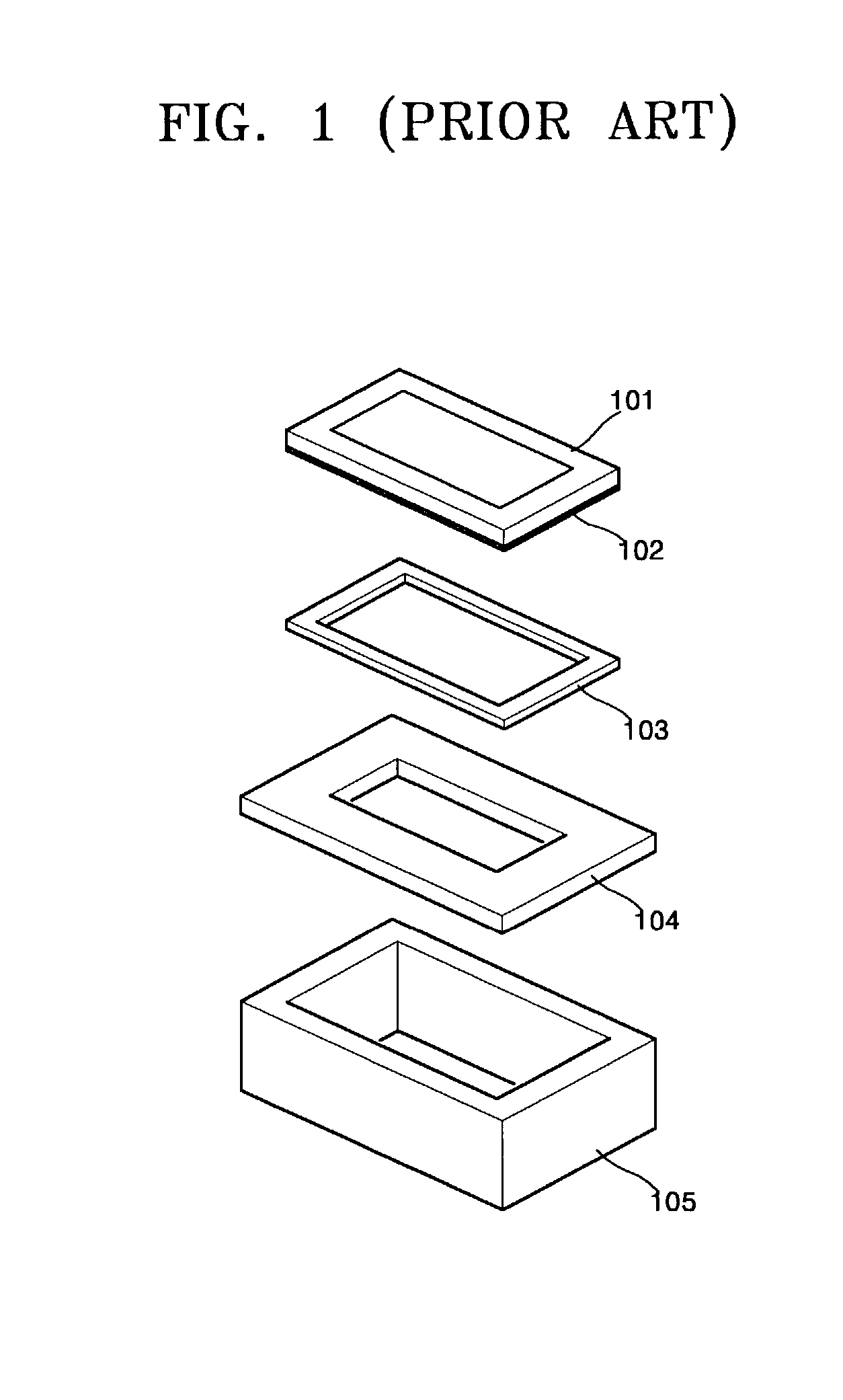
However, a device such as a micromirror that is employed in the MEMS has weak heat resistance properties and is very susceptible to an environment of adhesion due to water or by-products, and thus, taking into consideration the characteristics of the MEMS, the most appropriate sealing method must be selected.
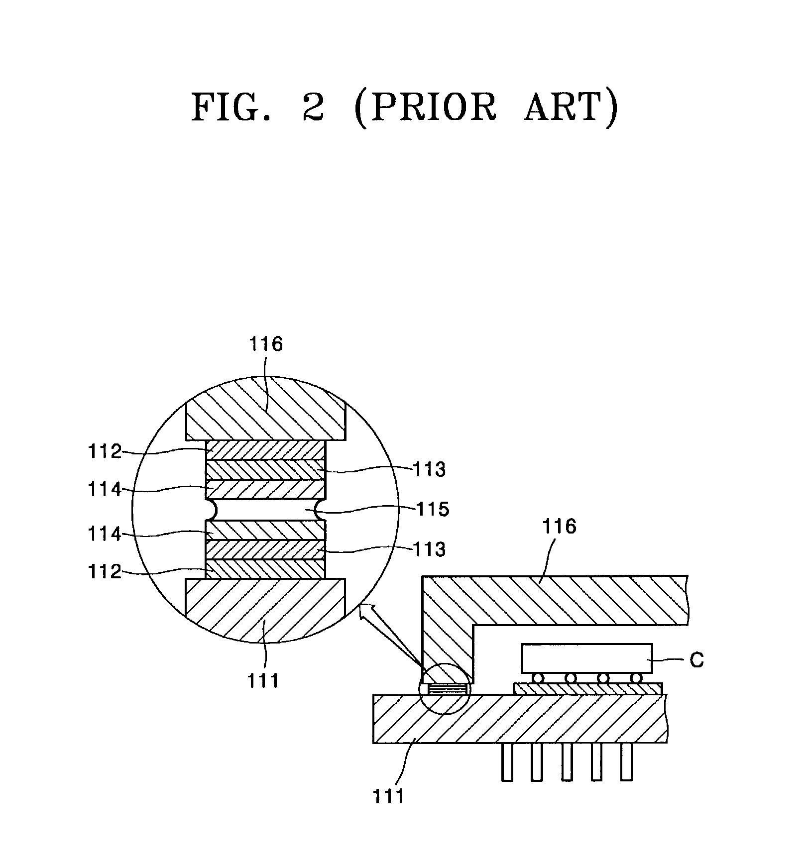
In the anodic bonding method and the glass frit bonding method, the sealing is performed at a high temperature of over 400° C. As described previously, the device such as a micromirror that is employed in the MEMS has very weak heat resistance properties, and thus, the anodic bonding method and the glass frit bonding method that are performed at a high temperature are not suitable for sealing the device.
In the adhesive bonding method, due to the penetration of water contained in an adhesive as well as water penetrated from an external environment, perfect hermetic sealing is not possible.
In the seam welding method, damages to a device due to heat can be comparatively reduced, and hermetic sealing is possible, but the components and the facilities required for the seam welding method are costly.
On the other hand, in the sealing method by Sn—Pb soldering, hermetic sealing is possible at a comparatively low price, but Sn—Pb is melted at a comparatively high temperature (about over 183° C.) in a MEMS manufacturing process, and wetting defects due to an oxide layer that is formed in the MEMS manufacturing process become sealing defects, and an environmental problem due to a Pb component occurs.
The process is very complicated and costly to manufacture.
However, a Pb or Cd-family solder contaminates an environment, and thus, Pb-free solder has been widely used.
However, the Pb-free solder is easily oxidized after deposition or during sealing, and thus, in order to prevent this, the Pb-free solder must be etched with a strong acid such as HCL, or dry-etched.
Thus, the manufacturing process becomes complicated.
The difficulty in manufacturing is that the Pb-free solder must be immediately sealed so as to prevent the Pb-free solder from being re-oxidized after etching.
Also, defects may occur in a device after sealing due to water or a by-product, which is generated during etching.
Further, when the Pb-free solder is heated at a high temperature during sealing, an oxide layer is formed, and thereby, defects in wetting, voids and cracks occur and a perfect hermetic sealing cannot be performed.
A flux is used to remove the oxide layer, but the flux is formed of acid rosin, and thus oxidizes and damages Al and other corrosive metals of a MEMS, and thus, adhesion occurs due to a by-product generated by the flux.
However, since this method also uses the Pb-free solder, problems due to oxidation described earlier remain.

Method used


Image

  • Low temperature hermetic sealing method having passivation layer
  • Low temperature hermetic sealing method having passivation layer
  • Low temperature hermetic sealing method having passivation layer

Examples


Embodiment Construction

[0028]The present invention will now be described in detail by describing illustrative, non-limiting embodiments thereof with reference to the accompanying drawings. In the drawings, the same reference characters denote the same elements.

[0029]FIG. 4 shows a low temperature hermetic sealing method having a passivation layer according to the present invention includes forming a package base 1 with a chip die 3 on which a micro-electromechanical system (MEMS) device 4 is disposed. Also, FIG. 4 shows forming a lid 15, which is to be disposed on the package base 1 to form a cavity 11, and sealing the package base 1 and the lid 15.

[0030]A junction layer 5 and a wetting layer 6 are deposited on a lid frame 2, and a solder layer 7, which is melted at a sealing temperature, serves as a sealant and thereby is maintained in a sealed state with layers contacting both sides of the solder layer 7, and a first protection layer 8 for preventing the oxidation of the solder layer 7 after deposition ...


PUM

PropertyMeasurementUnit
Temperatureaaaaaaaaaa
Wetting tensionaaaaaaaaaa

Abstract

A hermetic sealing method, which is capable of preventing oxidation of a micro-electromechanical system (MEMS) and sealing the MEMS at a low temperature. A low temperature hermetic sealing method having a passivation layer includes depositing a junction layer, a wetting layer, and a solder layer on a prepared lid frame, depositing a first protection layer for preventing oxidation on the solder layer and forming a lid, preparing a package base on which a device is disposed, and in which a metal layer and a second protection layer are formed around the device, and assembling the lid and the package base, heating, and sealing them. The protection layer is laminated on the solder layer that is formed by the lid, thereby preventing oxidation without using a flux. The low temperature hermetic sealing method having a passivation layer is suitable for sealing a device, such as the MEMS, which is sensitive to heat, water and other by-products.

Description

BACKGROUND OF THE INVENTION[0001]1. Field of the Invention[0002]The present invention relates to a hermetic sealing method and, more particularly, to a hermetic sealing method, which is capable of preventing oxidation of a micro-electromechanical system (MEMS) and sealing the MEMS at a low temperature.[0003]This application is based on Korean Patent Application No. 2001-76235 filed on Dec. 4, 2001, the disclosure of which is incorporated herein by reference in its entirety.[0004]2. Description of the Related Art[0005]In general, a micro-electromechanical system (MEMS) is manufactured through photolithography, deposition, and etching after a very thin metal layer or a thin film, such as oxide and polymer, is laminated on a silicon substrate. The MEMS is very thin and microscopic, and thus is very sensitive to the environments of high temperature, fine dust, water or gas. In particular, a capillary phenomenon due to water or by-products, and a surface force, such as Van der Waals forc...

Claims


Application Information

Patent Timeline
IPC IPC(8): H05K3/30B81C3/00B81B7/00B81C1/00H01L21/50H01L23/02H01L23/10
CPCB81C1/00269H01L23/10H01L24/97H01L21/50Y10T29/49789H01L2224/16225H01L2224/48091H01L2224/48227H01L2924/01004H01L2924/01013H01L2924/01027H01L2924/01029H01L2924/0103H01L2924/01046H01L2924/01047H01L2924/01049H01L2924/01051H01L2924/01075H01L2924/01078H01L2924/01079H01L2924/01082H01L2924/01322H01L2924/09701H01L2924/15153H01L2924/15165H01L2924/15312H01L2924/16152H01L2924/163Y10T29/49144H01L2924/01005H01L2924/01006H01L2924/01024H01L2924/01033H01L24/48Y10T29/49794Y10T29/4913Y10T29/49146Y10T29/49002H01L2924/00014H01L2224/45099H01L2224/85399H01L2924/12042H01L2924/16195H01L2924/00H01L2224/45015H01L2924/207B81C1/00
Inventor KIM, WOON-BAESHIN, HYUNG-JAECHO, CHANG-HOKANG, SEUNG-GOO
Owner SAMSUNG ELECTRONICS CO LTD
Learn More