OLEDs having n-type doping

a technology of n-type and n-type, applied in the direction of discharge tube luminescnet screen, other domestic articles, natural mineral layered products, etc., can solve the problems of limiting the conductivity of the layer, low number of charge carriers, and doping with li

Inactive Publication Date: 2006-07-04
SOUTHERN CALIFORNIA THE UNIV OF
View PDF23 Cites 60 Cited by
  • Summary
  • Abstract
  • Description
  • Claims
  • Application Information

AI Technical Summary

Problems solved by technology

In layers comprising organic materials and metal complexes, the number of charge carriers may be very low, significantly limiting the conductivity of the layer.
However, there are two potential drawbacks of doping with Li.
The first drawback of Li doping is that the number of free carriers generated by Li doping is far less than the amount of Li that is doped into the film (carriers / Li<10%).
A second problem of Li doping is that Li may be highly mobile, readily diffusing throughout a device.
Li diffusion into layers that are not meant to be redox doped leads to marked degradation of device performance due to the formation of trapping or quenching sites.
Clearly the problems with Li doping are related to its high charge density and small size.

Method used

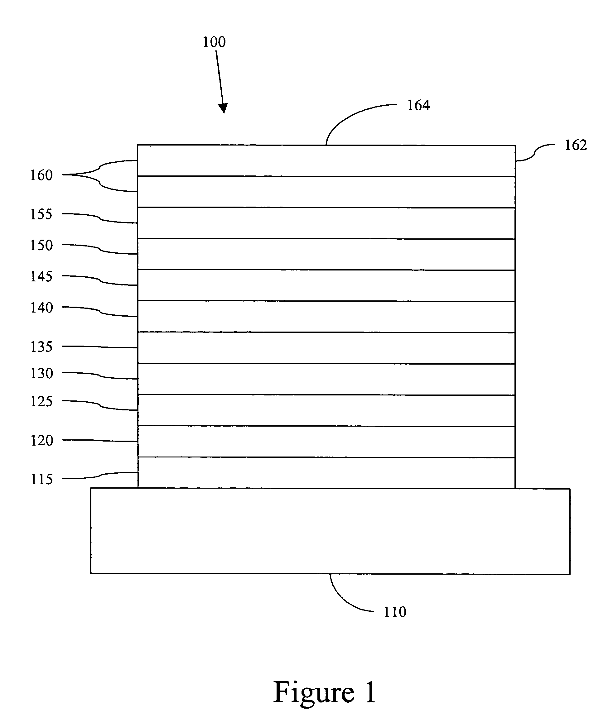
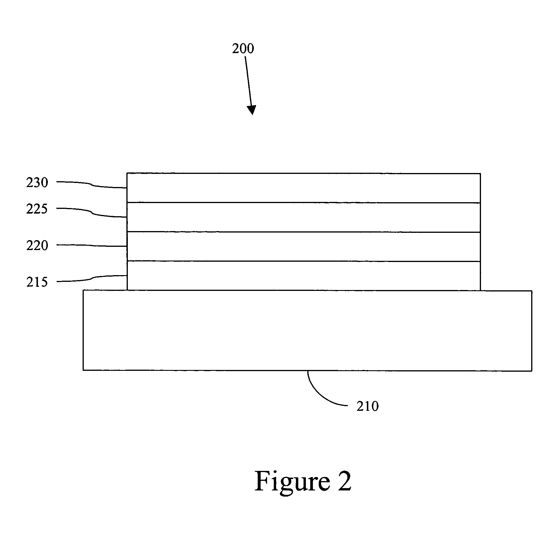

Image

  • OLEDs having n-type doping
  • OLEDs having n-type doping
  • OLEDs having n-type doping

Examples


example 1

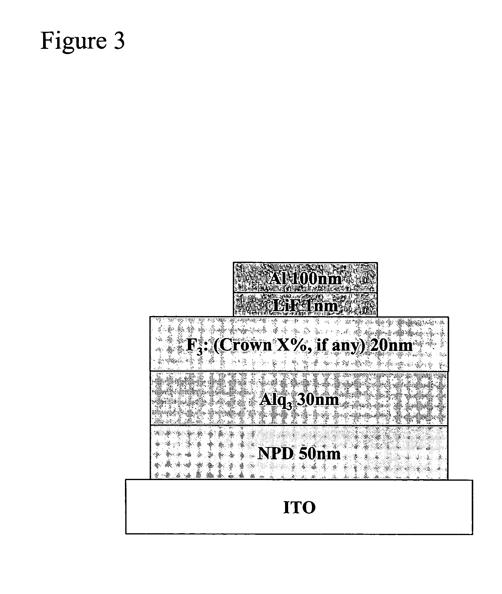
[0114]Two devices were prepared, ITO / NPD (500 Å) / Alq3 (300 Å) / F3 (200 Å) / Li (10 Å) / Al (1000 Å) and ITO / NPD (500 Å) / Alq3 (300 Å) / F3+15% DBC (200 Å) / Li (10 Å) / Al(1000 Å). The organic light emitting devices were grown on a glass substrate pre-coated with a ˜100-nm thick layer of indium-tin-oxide (ITO) having a sheet resistance of ˜20 Ω / □. Substrates were cleaned with solvents and then cleaned by exposure to UV-ozone ambient for 10 minutes. After cleaning, the substrates were immediately loaded into a thermal evaporation system operating at a base pressure of ˜1×10⁻⁶ Torr. A 500-Å-thick 4–4′-bis[N-(1-naphthyl)-N-phenyl-amino]biphenyl (α-NPD) hole transport layer (HTL) was deposited. Next, a 300-Å-thick aluminum (III) tris (8-hydroxyquinoline) (Alq3) as emitting material was deposited. Dibenzo-18-crown-6 (15% by weight) was co-deposited with fluorene trimer (F3) to form the 300-Å-thick electron transport layer (ETL) and in the reference device only F3 was deposited as ETL. Device cathode...

example 2

[0117]Devices were prepared having the structure ITO / NPD (500 Å) / Alq3 (300 Å) / F3 (200 Å) / Li (10 Å) / Al (1000 Å) and ITO / NPD (500 Å) / Alq3 (300 Å) / ETL (200 Å) / Li(10 Å)Al (1000 Å), in which ETL is (i) 5% DBC in F3, (ii) 15% DBC in F3, (iii) 25% DBC in F3, or (iv) F3 alone. Organic light emitting devices were grown on a glass substrate pre-coated with a ˜100-nm thick layer of indium-tin-oxide (ITO) having a sheet resistance of ˜20 Ω / □. Substrates were cleaned with solvents and then cleaned by exposure to UV-ozone ambient for 10 minutes. After cleaning, the substrates were immediately loaded into a thermal evaporation system operating at a base pressure of ˜1×10⁻⁶ Torr. A 500-Å-thick 4–4′-bis[N-(1-naphthyl)-N-phenyl-amino]biphenyl (α-NPD) hole transport layer (HTL) was deposited. Next, a 300-Å-thick aluminum (III) tris (8-hydroxyquinoline) (Alq3) as emitting material was deposited. In three separate devices, a 300-Å-thick electron transport layer (ETL), consisting of X % (X %=5%, 15% and ...

example 3

[0119]Devices were prepared having the structures (A) ITO / NPD (400 Å) / mCP(100 Å) / 10% Ir(4,6-F2 ppy)2(BPZ4): p-(SiPh3)2Ph (250 Å) / F3 (200 Å) / 15% F3:DBC (100 Å) / LiF / Al (1000 Å), and (B) ITO / NPD (400 Å) / 10% Ir(4,6-F2 ppy)2(BPz4): p-(SiPh3)2Ph (250 Å) / F3 (200 Å) / 15% F3:DBC (100 Å) / LiF / Al (1000 Å) (FIGS. 12A and 12B). The organic light emitting devices were grown on a glass substrate pre-coated with a ˜100-nm thick layer of indium-tin-oxide (ITO) having a sheet resistance of ˜20 Ω / □. Substrates were cleaned with solvents and then cleaned by exposure to UV-ozone ambient for 10 minutes. After cleaning, the substrates were immediately loaded into a thermal evaporation system operating at a base pressure of ˜1×10⁻⁶ Torr. A 500-Å-thick 4–4′-bis[N-(1-naphthyl) -N-phenyl-amino]biphenyl (α-NPD) hole transport layer (HTL) was deposited. In one device a 100 Å thick layer of mCP was deposited. Next a 250-Å-thick phosphorescent emissive layer of 10% Ir(4,6-F2 ppy)2(BPz4) in p-(SiPh3)2Ph (250 Å) was ...


PUM

PropertyMeasurementUnit
quantum efficiencyaaaaaaaaaa
timeaaaaaaaaaa

Abstract

The present invention provides an organic light emitting device comprising an anode, a cathode, and an organic layer disposed between the anode and the cathode, wherein the organic layer comprises a host material, an alkali metal or an alkaline earth metal, and a metal binding agent. In a preferred embodiment, the organic layer is an electron transport layer in which the metal binding agent may confine the alkali metal or the alkaline earth metal.

Description

RESEARCH AGREEMENTS[0001]The claimed invention was made by, on behalf of, and / or in connection with one or more of the following parties to a joint university-corporation research agreement: Princeton University, The University of Southern California, and Universal Display Corporation. The agreement was in effect on and before the date the claimed invention was made, and the claimed invention was made as a result of activities undertaken within the scope of the agreement.FIELD OF THE INVENTION[0002]The present invention relates to organic light emitting devices (OLEDs), and more specifically to OLEDs using improved n-type doping.BACKGROUND[0003]Opto-electronic devices that make use of organic materials are becoming increasingly desirable for a number of reasons. Many of the materials used to make such devices are relatively inexpensive, so organic opto-electronic devices have the potential for cost advantages over inorganic devices. In addition, the inherent properties of organic ma...

Claims


Application Information

Patent Timeline
Patent Type & Authority Patents(United States)
IPC IPC(8): H05B33/12C09K11/06H01L51/00H01L51/50H05B33/14
CPCC09K11/06H01L51/002H01L51/5048H05B33/14H01L51/005C09K2211/1048C09K2211/1088C09K2211/181H01L51/0039Y10S428/917H01L51/0081H01L51/009H01L51/0094H01L2251/308H10K71/30H10K85/115H10K85/60H10K85/361H10K85/324H10K85/40H10K50/14H10K2102/103
Inventor THOMPSON, MARK E.GARON, SIMONA
Owner SOUTHERN CALIFORNIA THE UNIV OF
Why Eureka
Try Eureka