Method for determining cell body and biasing plate contact locations for embedded dram in SOI

a technology of biasing plate and soi, which is applied in the field of determining the contact location of the cell body and the biasing plate of the embedded dynamic random access memory (edram), can solve the problems of parasitic paths and junction capacitance problems, memory cell information can lose information, and the amount of surface area is needed

Inactive Publication Date: 2006-07-04
IBM CORP
View PDF11 Cites 11 Cited by
  • Summary
  • Abstract
  • Description
  • Claims
  • Application Information

AI Technical Summary

Problems solved by technology

Due to charge leakage, the capacitor discharges gradually and the memory cell can lose the information.
A relatively large amount of surface area is needed for the electrical isolation of the various FETs, which is undesirable in the current trend toward overall size reduction and greater integration.
Additionally, parasitic paths and junction capacitance problems may be present because of the physical proximity of the source / drain diffusions to other FETs and to the bulk substrate.
These problems more frequently arise when trying to scale circuitry down to the sizes necessary for greater circuit density.
However, SOI devices may suffer from problems such as self-heating, electrostatic discharge susceptibility, low breakdown voltage, and dynamic floating body effects, which in turn present problems for passgate devices and devices requiring tight threshold voltage control.
The floating body effect greatly affects device reliability.
Certain types of semiconductor memory are more susceptible to the floating body effect.
Thus, in DRAM, the floating body effect is especially detrimental since it is critical that the associated transistor stays in an “off” condition to prevent charge leakage from the storage capacitor.
However, the additional lithography, patterning and implantation steps associated therewith increase the overall manufacturing costs of the device.

Method used


Image

  • Method for determining cell body and biasing plate contact locations for embedded dram in SOI
  • Method for determining cell body and biasing plate contact locations for embedded dram in SOI
  • Method for determining cell body and biasing plate contact locations for embedded dram in SOI

Examples


Embodiment Construction

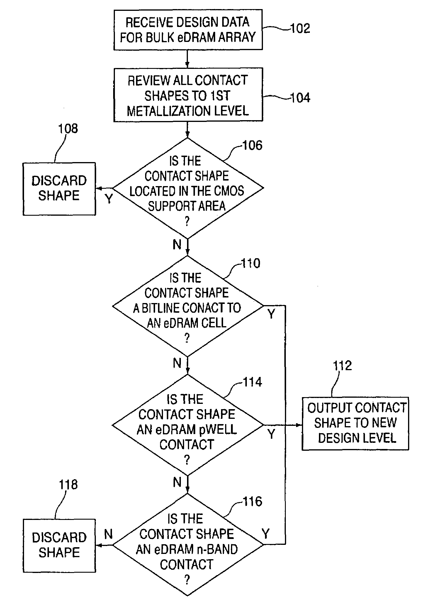
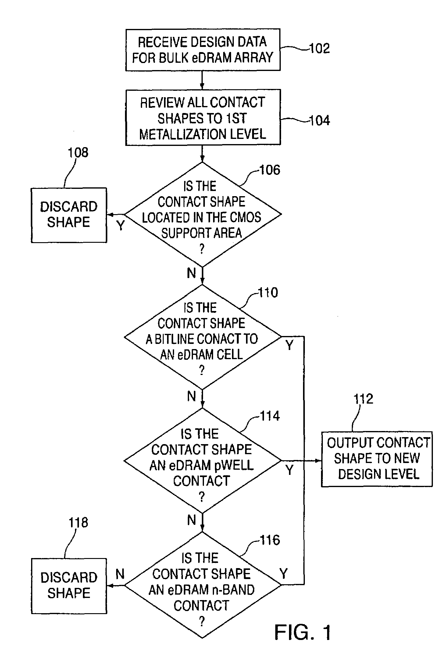
[0013]Disclosed herein is a method for determining cell body and biasing plate contact location for embedded dynamic random access memory (eDRAM) in silicon-on-insulator (SOI) substrates. Briefly stated, the method utilizes an algorithm developed to allow body contacts to be designed and incorporated into the cells (as well as the periphery) of an eDRAM array using existing eDRAM bulk design data and real estate. In particular, the algorithm analyzes the shape and location of each contact in the bulk eDRAM design data from the first level of metallization to silicon or polysilicon. Within the vast number of total contacts at this level, those existing contacts that do not define suitable locations for SOI body contacts (e.g., contacts in the support areas of the device) are automatically filtered out. Moreover, those existing contacts that do define suitable locations for SOI body contacts (e.g., bitline to eDRAM cell contacts, periphery p-well contacts or n-band contacts) are affir...


PUM


Abstract

A method for determining contact location for embedded dynamic random access memory (eDRAM) formed in a silicon-on-insulator (SOI) substrate includes reviewing contact design data for an eDRAM device and discarding contact locations corresponding to contact shapes within a support area of the eDRAM device. Contact locations corresponding to bitline contacts to storage cells within the eDRAM device are saved and outputted to a custom design level to be used in forming body contacts for the eDRAM formed in the SOI substrate.

Description

BACKGROUND OF INVENTION[0001]The present invention relates generally to semiconductor device processing and, more particularly, to a method for determining cell body and biasing plate contact location for embedded dynamic random access memory (eDRAM) in silicon-on-insulator (SOI) substrates.[0002]Dynamic random access memory, or DRAM, is a type of semiconductor memory in which the information is stored as data bits in capacitors on a metal-oxide-semiconductor (MOS) integrated circuit. Each bit is typically stored as an amount of electrical charge in a storage cell consisting of a capacitor and a transistor. Due to charge leakage, the capacitor discharges gradually and the memory cell can lose the information. Therefore, to preserve the information, the memory must be refreshed periodically. Despite this inconvenience, the DRAM is a very popular memory technology because of its high density and consequent low price.[0003]Conventional semiconductor DRAM devices are formed in bulk semi...

Claims


Application Information

Patent Timeline
Patent Type & Authority Patents(United States)
IPC IPC(8): G06F17/50H01L21/8242H01L21/84H01L27/02H01L27/12
CPCG06F17/5068H01L21/84H01L27/1203H01L27/10861H01L27/10894H01L27/0214G06F30/39H10B12/038H10B12/09
Inventor BARD, KAREN A.HO, HERBERT L.
Owner IBM CORP
Why Eureka
Try Eureka