Monolithic class D amplifier

a technology of monolithic amplifiers and amplifiers, applied in the direction of low frequency amplifiers, gated amplifiers, electrical transducers, etc., can solve the problems of reducing the efficiency of the amplifier, affecting the operation of the amplifier, and shortening the short circuit of two transistors across the load, so as to reduce the pinching effect, maximize the specific channel width, and minimize the cell area

Inactive Publication Date: 2006-07-11
INTERSIL INC
View PDF21 Cites 64 Cited by
  • Summary
  • Abstract
  • Description
  • Claims
  • Application Information

AI Technical Summary

Benefits of technology

[0043]The power MOS switch of the invention further comprises a drain contact situated within each drain region and a source contact situated in each of the areas of intersection of the narrow elongated source distribution region with the transverse narrow branch regions. This configuration serves to minimize cell area while maximizing specific channel width.
[0044]The invention provides a quasi-vertical DMOS transistor (QVDMOS) together with a method for its manufacture either alone or in combination with other transistors such as PMOS transistors, NMOS transistors and bipolar transistors. The QVDMOS transistor is constructed on the substrate of a first type of conductivity, usually P-type material. The substrate has a highly doped buried layer of a second or N-type conductivity. An epitaxial layer is disposed above the buried layer and comprises a light doping of a second or N-type conductivity. A drain sinker region of heavily doped second or N-type conductivity extends from the surface of the epitaxial layer to the buried layer. A body region of a first or P-type conductivity is formed in the surface of the epitaxial layer and space from the drain. A source region, preferably an annular source region, is formed in the body region. The source region is formed with a shallow implant of a second or N-type conductivity and has a relatively shallow depth. A body tie is formed in the opening in the source region and has a first or P-type conductivity. The depth of the body tie is slightly greater than the depth of the source region. The body tie extends beneath the source region but not beyond the source region and thereby reduces the pinching effect between the N epi layer and the N-type source region. A gate is disposed over the source region of the body region for selectively establishing a current path from the drain to the source. The gate is provided with sidewall spacers that are used to position the body tie diffusion so that the outer limits of the body

Problems solved by technology

Likewise, further logic circuitry monitors the operating voltage of the power QVDMOS devices and inhibits their operation if there is ins

Method used


Image

  • Monolithic class D amplifier
  • Monolithic class D amplifier
  • Monolithic class D amplifier

Examples


embodiment 1

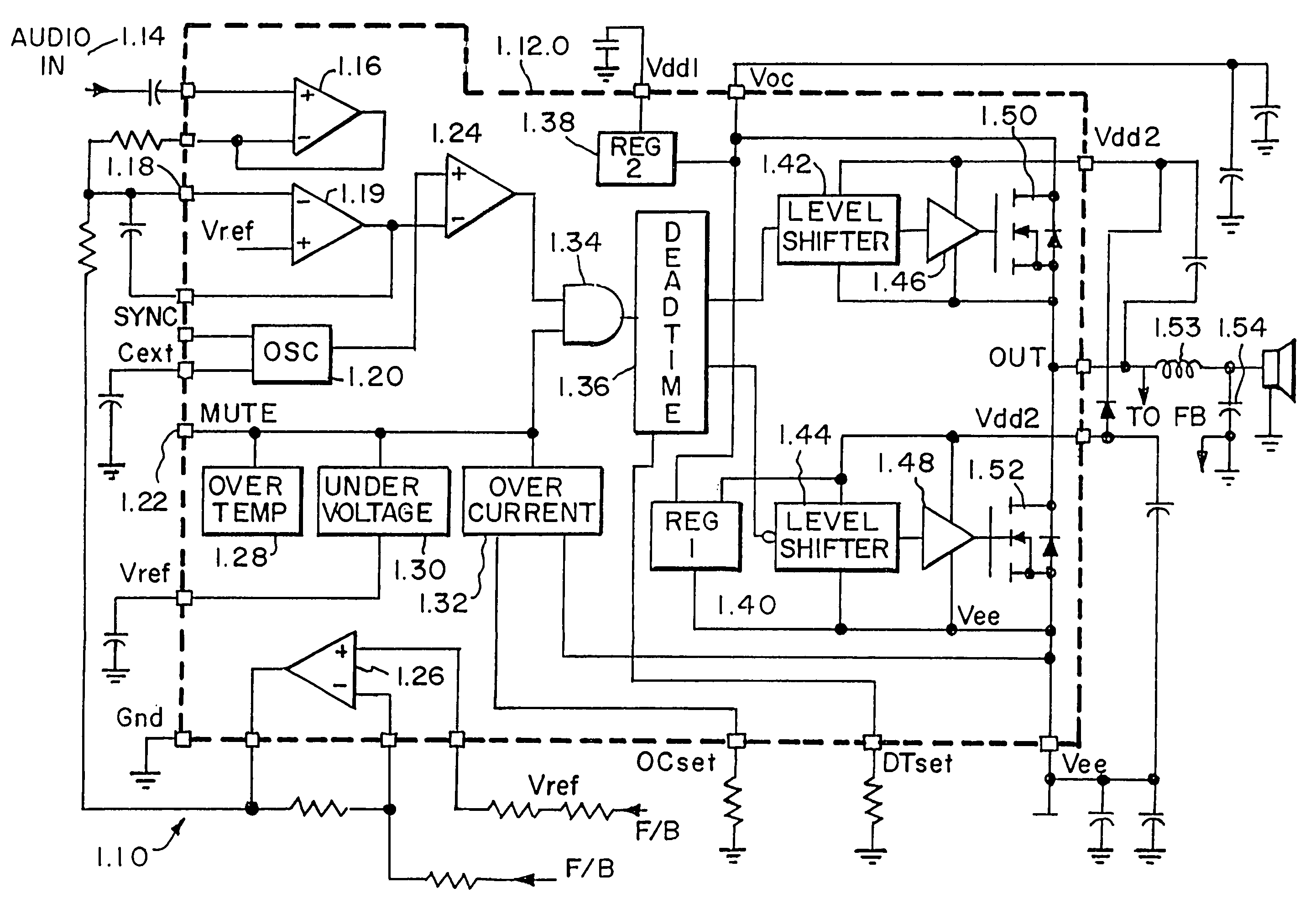
[0101]The first embodiment of the invention is shown in FIG. 1J. Analog switch S1 has been added to the integrator circuit A1. Switch S1 is controlled by the disable signal. When the output bridge is disabled, the S1 switch is closed and A1 becomes a summing amplifier instead of an integrator. Since the bridge is not switching, the voltage across the speaker drops to zero, and the output of A2 goes to +6V. In this configuration A1 is an inverting amplifier with a gain of −R3 / R2 times the input. R3 is chosen here so that A1 does not saturate prior to start-up. So, when the amplifier is enabled, the bridge starts switching and switch S1 is opened. The error voltage output of A1 continues to follow the input as it was before S1 was opened, eliminating the start-up thump.

embodiment 2

[0102]The second embodiment of the invention is shown in FIG. 1K and further in FIGS. 1L and 1M. This embodiment relates to audio IC PWM controllers where the integration amplifier A1 is external to the IC.

[0103]Referring to FIG. 1K, when the IC U3 is disabled, the switching of the output stops. S3 connects the mute signal to ground which controls switch S2 so that the + input to the PWM comparator is connected to +6V. When the disable signal is removed, switch S3 allows a current source to charge a capacitor on the mute node and cause a slowly moving control voltage at switch S2. While the control voltage is low, the output begins to switch since the part is enabled. The PWM comparator commands a 50% square wave regardless of the error signal because the + input to the comparator is at +6V, the midpoint of the triangle wave on the − input of the comparator. The 50% duty cycle output of the H-Bridge is filtered to result in zero voltage across the load. As the control voltage rises,...


PUM


Abstract

A monolithic 1.75 is mounted in a speaker cabinet 1.71 to drive the voice coil 1.74 of the speaker 1.70. The monolithic integrated circuit may be a class D amplifier 1.10, and is at least a half-bridge or full bridge power MOSFET device. Structures and process for forming the mos switching devices 2.20 of the bridge driver circuits are disclosed. Also disclosed is the N+ buried layer 4.14 of the QVDMOS transistors 4.43 of the bridge circuits.

Description

CROSS REFERENCE TO RELATED APPLICATIONS[0001]This application is a continuation of U.S. patent application Ser. No. 09 / 392,806 filed Sep. 9, 1999 now abandoned which is a divisional application of U.S. application Ser. No. 08 / 973,769, filed Dec. 11, 1997 now U.S. Pat. No. 5,973,368, which is a 371 of International Application No. PCT / US96 / 08826 filed on Jun. 5, 1996.INTRODUCTIONAudio Amplifiers[0002]A convention push-pull (class AB) linear amplifier (FIG. 1A) modulates load power by continuously varying conduction through its pass elements during most, if not all, of the conduction cycle. Q1 conducts during the positive half-cycle, and Q2 conducts during the negative. During each half-cycle, the conducting transistor operates in its linear region. The transistor must supply the required current to the load while reducing the voltage between the supply and the load. The power dissipated in the transistor, which equals VBUS−VLOAD)×ILOAD, is wasted in the form of heat. Q1 and Q2 have l...

Claims


Application Information

Patent Timeline
IPC IPC(8): H03F21/00H01L29/76H03F3/217H03F3/38H04R3/00H03F99/00H01L21/8249H01L27/02H01L27/06H03F1/52
CPCH01L21/8234H03F3/72H01L27/0207H01L27/0623H01L27/0922H01L29/0696H01L29/4238H01L29/66719H01L29/7809H01L29/7811H01L29/7815H03F1/523H03F3/187H03F3/217H03F3/2171H03F3/2173H01L21/8249H01L29/0615H01L29/1095H01L29/456H01L29/665
Inventor PEARCE, LAWRENCE G.HEMMENWAY, DONALD F.
Owner INTERSIL INC
Why Eureka
Try Eureka