Wavelength variable light source

a light source and variable technology, applied in the field of light sources, can solve the problems of difficult to modulate the width of the light emitting spectrum is great, and it is difficult to use the light source, so as to achieve the effect of narrowing the width of the light emitting spectrum and easily changing the light emitting wavelength

Inactive Publication Date: 2006-07-18
SANYO ELECTRIC CO LTD
View PDF11 Cites 12 Cited by
  • Summary
  • Abstract
  • Description
  • Claims
  • Application Information

AI Technical Summary

Benefits of technology

[0006]A first object of the present invention is to provide a wavelength variable light source which has a narrow width of a light emitting spectrum and can readily vary a light emitting wavelength in the light source for allowing organic substance of an organic EL element or the like to emit light.
[0007]A second object of the present invention is to provide a wavelength variable light source which can widen an angle of view and limit the same for protection of an privacy.
[0008]The wavelength variable light source according to the present invention comprises: a light emitting layer containing therein light emitting substance having a carbon-carbon inter-atomic bond; a pair of electrodes disposed on both sides of the light emitting layer while holding the light emitting layer therebetween; a pair of main reflectors disposed on both sides of the light emitting layer while holding the light emitting layer therebetween, so as to constitute an optical resonator with respect to light emitted from the light emitting layer; and refractive index modulating means disposed on the optical path of the optical resonator, wherein the refractive index modulating means can reversibly vary the length of the optical path of the optical resonator so as to control the wavelength and / or directivity of the light emitted from the light source.
[0009]Examples of the refractive index modulating means according to the present invention include means consisting of a piezoelectric member held between the pair of electrodes. With the application of a voltage to the piezoelectric member by the pair of electrodes, the thickness of the piezoelectric member is varied by a piezoelectric effect, so that its refractive index can be varied. The above-described piezoelectric member is provided on the optical path of the optical resonator, thereby varying the length of the optical path of the optical resonator, so as to control the variations of the length of the wavelength of the light emitted from the light source.
[0014]According to the present invention, it is preferable that the length of the optical path from the center of a region in the light emitting layer, in which the light emission occurs most strongly, to the main reflector should be substantially equal to a multiple of a natural number of a half of a predetermined peak wavelength of the light emitted from the light source. Specifically, for example, it is preferable that the length of the optical path from the center of a region in the light emitting layer, in which the light emission occurs most strongly, to the main reflector should range from 99 / 200 to 101 / 200 of a multiple of a natural number of a predetermined peak wavelength of the light emitted from the light source. With this setting, it is possible to further enhance a wavelength selecting effect.
[0018]According to the present invention, an auxiliary electrode having light transmittance may be disposed outside of at least either one of the pair of electrodes holding the light emitting layer therebetween. Such an auxiliary electrode is disposed in such a manner as to be brought into contact with the electrode made of the metallic thin film, thereby constituting a composite electrode consisting of the electrode made of the metallic thin film and the auxiliary electrode. With the auxiliary electrode having the light transmittance, the thickness of the electrode made of the metallic thin film can be reduced, thereby achieving both characteristics of conductivity and light transmittance. Consequently, the light can be emitted on the side on which the above-described auxiliary electrode is disposed.

Problems solved by technology

In a light source for allowing the organic substance of the organic EL element or the like to emit light, it has been difficult to modulate a light emitting wavelength because the width of a light emitting spectrum has been great.
Consequently, it has been difficult to use the light source for allowing the organic substance of the organic EL element or the like to emit the light as a light source for performing optical communications at a high speed by a frequency modulating system.
Furthermore, since a response speed during the flickering of the light source has ranged from several micro seconds to several hundred micro seconds, it has been difficult to perform the optical communications at the high speed even by a pulse width modulation system or a pulse code modulation system.

Method used


Image

  • Wavelength variable light source
  • Wavelength variable light source
  • Wavelength variable light source

Examples


example 1

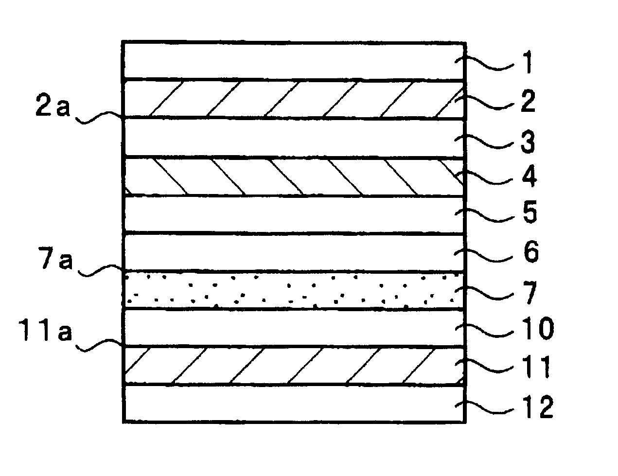
[0025]FIG. 1 is a schematic cross-sectional view showing a wavelength variable light source in a preferred embodiment according to the present invention. A thin film (having a thickness of 200 nm) made of gold serving as a first electrode 2 is formed on a substrate 1 made of glass by sputtering method. On the first electrode 2, a piezoelectric thin film 3 (having a thickness of 50 nm) having light transmittance is formed as refractive index modulating means by reactive sputtering method with an electron cyclotron resonance (abbreviated as “ECR”) plasma in an atmosphere of argon and nitrogen. The piezoelectric thin film 3 is made of aluminum nitride (AlN). On the piezoelectric thin film 3, a transparent conductive thin film made of In2O3—SnO2 (ITO) (having a thickness of 50 nm) is formed as a second electrode 4 by sputtering method.

[0026]On the second electrode 4, a hole injecting layer 5 (having a thickness of 9 nm) made of copper phthalocyanine (CuPc) expressed by the following che...

example 2

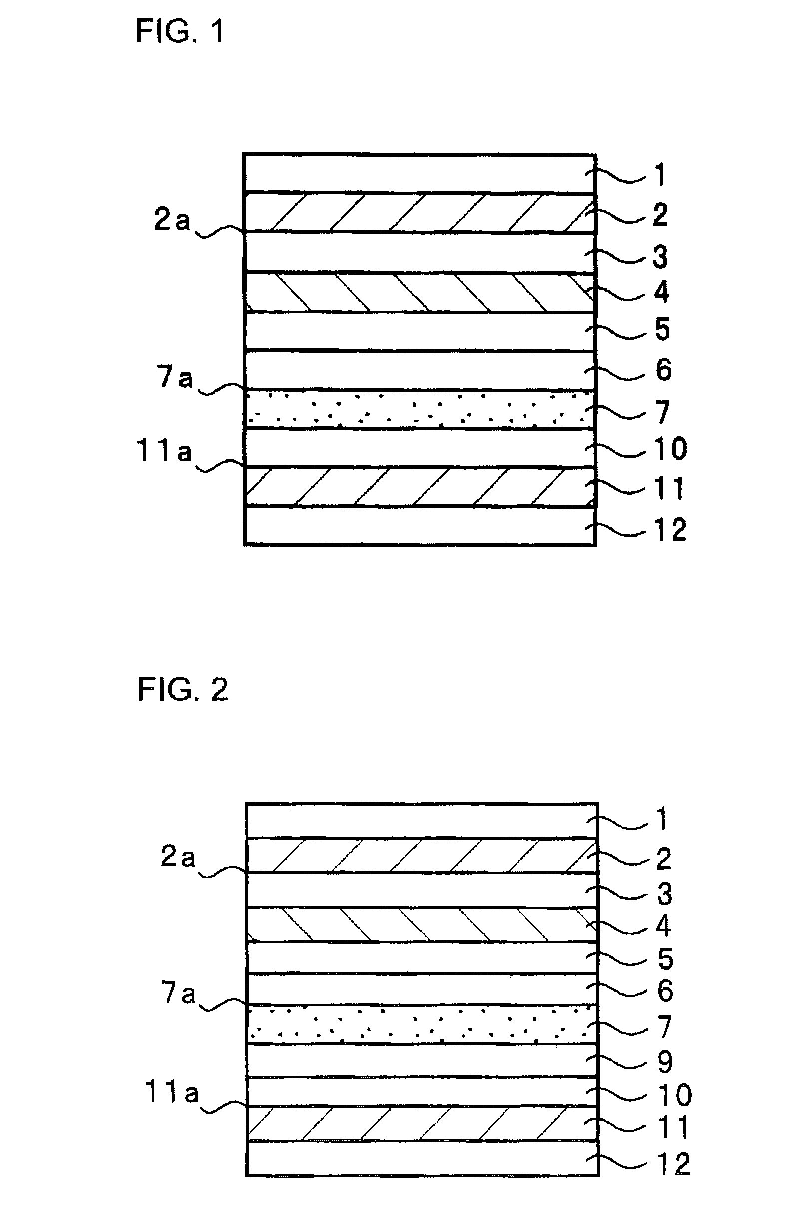
[0050]FIG. 2 is a schematic cross-sectional view showing a wavelength variable light source in another preferred embodiment. A thin film (having a thickness of 50 nm) made of gold serving as a first electrode 2 was formed on a (110) surface of a sapphire substrate serving as a substrate 1 by sputtering method. Subsequently, on the first electrode 2 was formed a thin film (having a thickness of 74 nm) as a piezoelectric thin film 3 made of zinc oxide (ZnO) by reactive sputtering method with an electron cyclotron resonance (abbreviated as “ECR”) plasma in an atmosphere of argon and oxygen. On the piezoelectric thin film 3, an ITO thin film (having a thickness of 50 nm) was formed serving as a second electrode 4 by sputtering method.

[0051]On the second electrode 4, the same hole injecting layer 5 and the same hole transporting layer 6, as those in Example 1, were formed.

[0052]On the hole transporting layer 6, a mixture light emitting layer (having a thickness of 35 nm) was formed by a ...

example 3

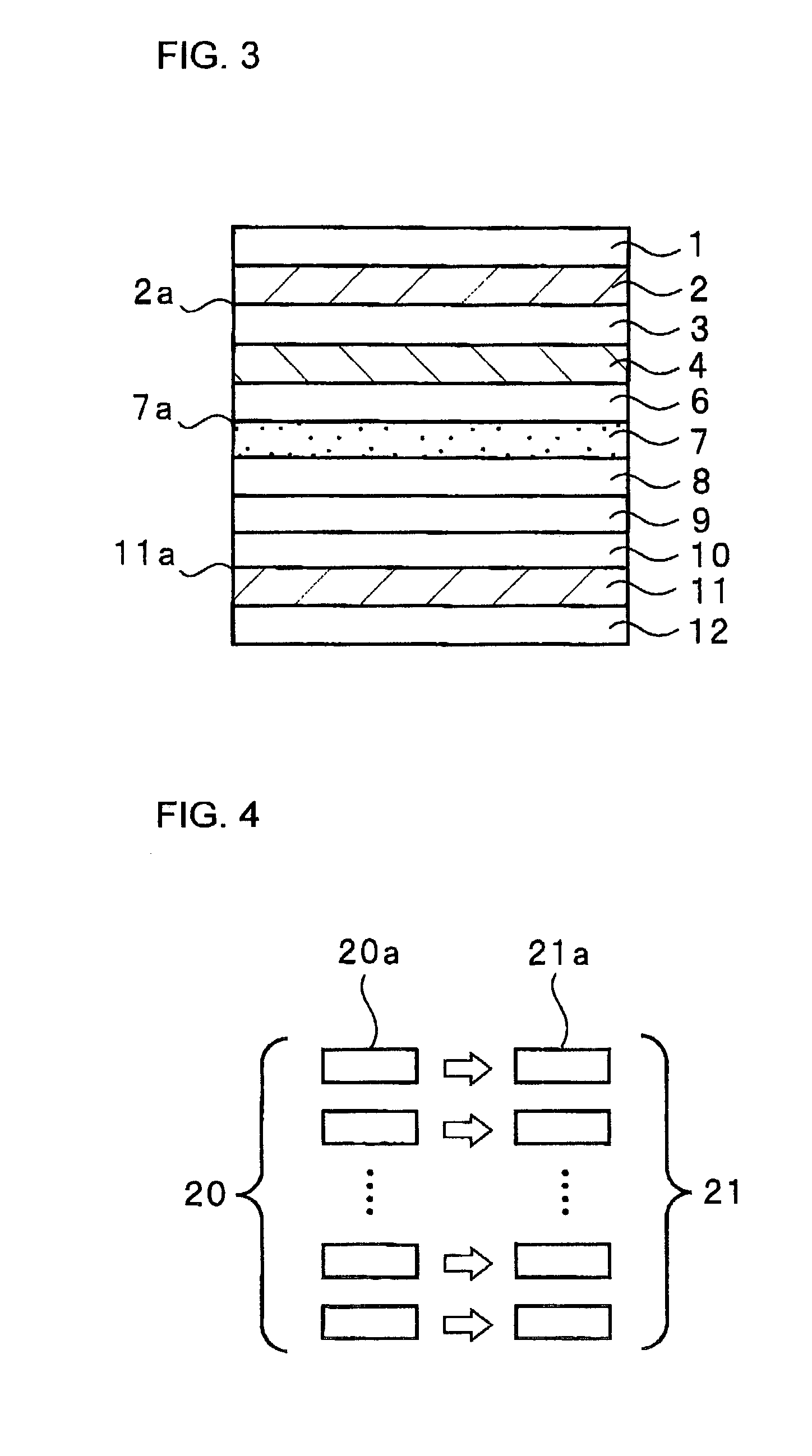
[0066]FIG. 3 is a schematic cross-sectional view showing a wavelength variable light source in a further preferred embodiment. A thin film (having a thickness of 50 nm) made of gold as a first electrode 2 was formed on a (110) surface of a sapphire substrate as a substrate 1 by sputtering method. Subsequently, on the first electrode 2, a thin film (having a thickness of 50 nm) made of zinc oxide (ZnO) was formed as a piezoelectric thin film 3 by the same reactive sputtering method as in Example 2. On the piezoelectric thin film 3, an ITO thin film (having a thickness of 48 nm) was formed as a second electrode 4 by sputtering method. Thereafter, a hole transporting layer 6 (having a thickness of 20 nm) made of NPB was formed.

[0067]On the hole transporting layer 6, a mixture light emitting layer (having a thickness of 30 nm) was formed as a light emitting layer 7 containing 94% by mass of 4,4′-bis(carbazol-9-yl)-biphenyl (CBP) expressed below by a chemical formula and 6.0% by mass of ...


PUM


Abstract

A wavelength variable light source is provided with: a light emitting layer containing therein light emitting substance having a carbon-carbon inter-atomic bond; a pair of electrodes disposed on both sides of the light emitting layer while holding the light emitting layer therebetween; a pair of main reflectors disposed on both sides of the light emitting layer so as to hold the light emitting layer therebetween, thereby to constitute an optical resonator with respect to light emitted from the light emitting layer; and refractive index modulating means disposed on the optical path of the optical resonator, wherein the refractive index modulating means can reversibly vary the length of the optical path of the optical resonator so as to control the wavelength of the light emitted from the light source.

Description

BACKGROUND OF THE INVENTION[0001]1. Field of the Invention[0002]The present invention relates to a light source capable of varying a light emitting wavelength in a light source including an organic electroluminescence (organic EL) element or the like.[0003]2. Related Art[0004]An organic EL element using an amorphous thin film made of organic substance has been actively developed in recent years. In a light source for allowing the organic substance of the organic EL element or the like to emit light, it has been difficult to modulate a light emitting wavelength because the width of a light emitting spectrum has been great. For example, in a light source disclosed in Japanese Patent Publication Laid-open No. 08-315983, a light emitting layer includes an organic light emitting material having a light emitting peak wavelength ranging from 450 nm to 570 nm and a half-value breadth ranging from 100 nm to 200 nm.[0005]Consequently, it has been difficult to use the light source for allowing...

Claims


Application Information

Patent Timeline
Patent Type & Authority Patents(United States)
IPC IPC(8): H05B33/22H01L51/00H01L51/30H01L51/50H01L51/52H05B33/24
CPCH05B33/24H01L51/5036H01L51/5203H01L51/5265H01L51/5275H01L51/0052H01L51/0059H01L51/0062H01L51/0078H01L51/0081H01L51/0084H01L2251/558H01L51/0085H10K85/615H10K85/631H10K85/649H10K85/311H10K85/341H10K85/324H10K85/342H10K50/125H10K50/805H10K50/852H10K50/858H10K2102/351
Inventor FUJII, HIROYUKI
Owner SANYO ELECTRIC CO LTD
Why Eureka
Try Eureka