Method for manufacturing a microlens substrate and method for manufacturing a liquid crystal panel

a microlens substrate and liquid crystal display technology, which is applied in the field of manufacturing a microlens substrate and a manufacturing method of a liquid crystal display, can solve the problems of not being able to use a UV-curable resin, unable to meet the requirements of liquid crystal display requirements, and other than the visible light transmittance (1), so as to improve heat resistance, light fastness, and good chemical resistance

Inactive Publication Date: 2006-08-08
SONY CORP
View PDF3 Cites 10 Cited by
  • Summary
  • Abstract
  • Description
  • Claims
  • Application Information

AI Technical Summary

Benefits of technology

[0025]According to these methods of manufacturing a microlens substrate and a liquid crystal panel, the microlens is formed by burying a lens-shaped curve formed in the transparent substrate with an inorganic material film, so that the microlens substrate can be constituted only by use of an inorganic material without use of a resin. Thus, a microlens substrate having good chemical resistance and light fastness can be obtained. In addition, the heat resistance is so improved that it becomes possible to perform steps having a thermal treatment, such as the step of forming a thin film transistor on a flattened or planarized inorganic material film. In this way, one is enabled to form a thin film transistor while registering against a microlens in high precision.

Problems solved by technology

Especially, in the 2P technique (b), the use of a UV-curable resin is essential therefor, and it is unavoidable to use a UV-curable resin.
Hence, it is the usual practice to search for a resin that meets such requirements as set out above and optimally design the shape of microlens according to the refractive index depending on the type of device, with the attendant problem that the selection of material is difficult.
Especially, where a resin for microlens is used as an adhesive or an adhesive resin used is of a type different from that of a microlens, the requirements other than the visible light transmittance (1) pose problems to all of actually existing liquid crystal displays.
However, it has now been experienced that a slight variation in performance of UV-IR cut filters permits such a non-negligible degree of resin degradation as to occur by the action of light of the component contained within the above-mentioned wavelength region.
Only slight dissolution in these solvents influences a voltage retention of LCD and contributes to ion conduction, thus bringing about the degradation of LCD.
Further, with respect to reliability (5), resins are usually not resistant to moisture.
The requirement (6) presents problem particularly on the difference in thermal expansion between a substrate material and a resin.
Usually, it is more difficult to make a deep lens.
When using etching or the like, uniformity and productivity are adversely influenced, and where a substrate size is increased for cost cutting, a difficulty is involved in the uniformisation of a lens shape.

Method used


Image

  • Method for manufacturing a microlens substrate and method for manufacturing a liquid crystal panel
  • Method for manufacturing a microlens substrate and method for manufacturing a liquid crystal panel
  • Method for manufacturing a microlens substrate and method for manufacturing a liquid crystal panel

Examples


embodiment 1

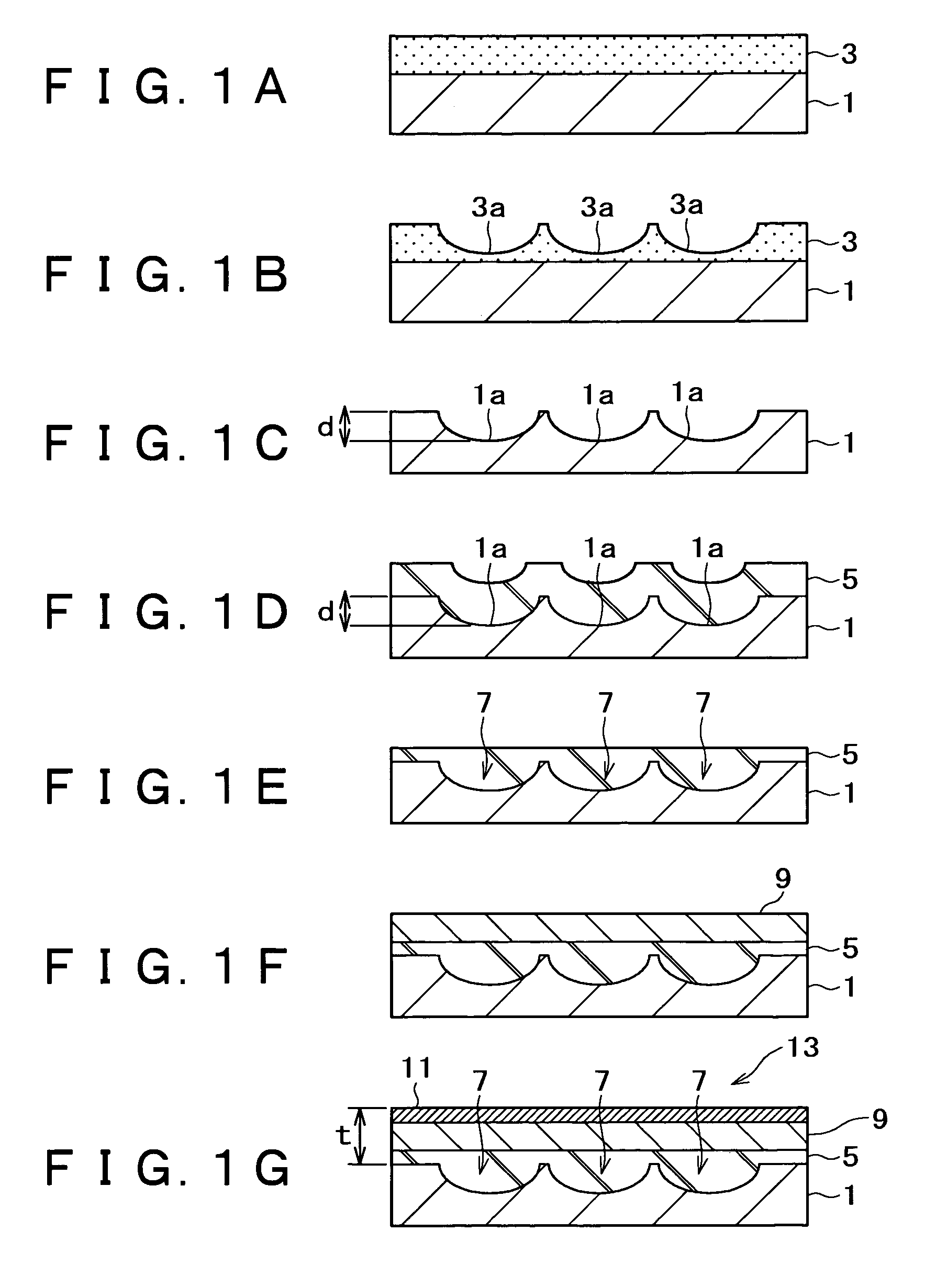
[0034]FIGS. 1A to 1B are, respectively, a sectional view illustrating a first example of a method of manufacturing a microlens substrate according to the invention. The first embodiment is illustrated with reference to these figures.

[0035]Initially, as shown in FIG. 1A, a resist film 3 is formed on a transparent substrate 1, which has, for example, a diameter of 6 inches and is made of fused silica (or Neoceram). In this case, the resist film 3 is formed in a thickness of 10 μm according to a spin coating technique.

[0036]Next, as shown in FIG. 1B, the resist film 3 is subjected to lithographic treatment at the surface side to form an array of lens-shaped concave curves which are a basic pattern of microlenses. In this embodiment, concave curves 3a are formed in the respective pixel regions of about 14 μm×14 μm created by partitioning a display region at the center of the surface side of the transparent substrate 1.

[0037]In this lithographic treatment, multiple exposure is carried ou...

embodiment 2

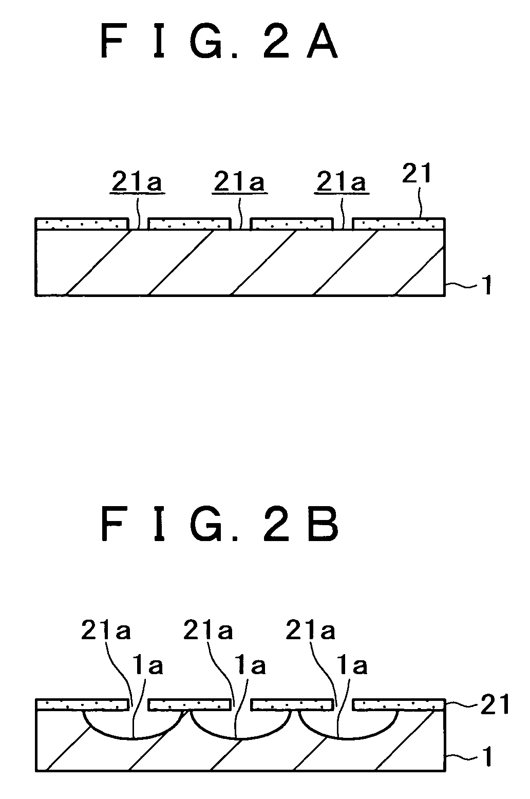
[0055]A second example of a method for manufacturing a microlens substrate according to the invention is illustrated with reference to FIGS. 2A and 2B which are, respectively, a sectional process view.

[0056]Initially, as shown in FIG. 2A, a resist pattern 21 is formed on a transparent substrate 1 similar to that used in the first embodiment by a lithographic technique. This resist pattern 21 has a hole 21a at the center of a lens-shaped concave curve to be formed, which is a basic pattern of a microlens.

[0057]Next, as shown inFIG. 2B, the transparent substrate 1 is isotropically etched through a mask of the resist pattern 21. This allows the isotropic etching to proceed around the hole 21a of the resist pattern 21, and concave curves 1a are formed in array within the respective pixel regions of a size of about 14 μm×14 μm formed by partitioning a display region at the center of the surface side of the transparent substrate 1. The respective concave curves 1a formed in this way are s...

embodiment 3

[0061]Next, a method for manufacturing a microlens substrate according to a third embodiment of the invention is illustrated with reference to FIGS. 3A to 3D which are, respectively, a sectional process view. It will be noted that these sectional process views corresponding to enlarged views of an essential part of FIGS. 1A to 1G and 2A to 2B.

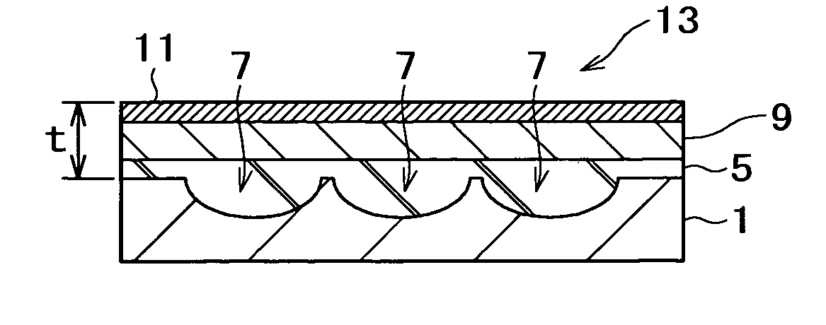
[0062]Initially, the steps illustrated with reference to FIGS. 1A to 1F in the first embodiment are, for example, carried out to form a microlens 7 wherein a concave curve 1a of a transparent substrate 1 is buried with an inorganic material film 5 as shown in FIG. 3A, and further to form a cover film 9. It will be noted that the procedure up to and including this step may be carried out by application of the procedure of the second embodiment.

[0063]Next, as shown in FIG. 3B, a light-shielding film pattern 31 is formed on the cover film 9. This light-shielding film pattern 31 is disposed at a position surrounding individual microlenses 7 or alon...


PUM

PropertyMeasurementUnit
wavelength regionaaaaaaaaaa
diameteraaaaaaaaaa
thicknessaaaaaaaaaa

Abstract

Disclosed herein is a method for manufacturing a microlens substrate which is excellent in chemical resistance and light fastness to intense light irradiation, and is capable of forming a microlens substrate of a high accuracy of form. The method includes the steps of: forming a lens-shaped curve at a surface side of a transparent substrate; forming an inorganic material film on the transparent substrate so as to bury the curve therewith; and planarizing the surface of the inorganic material film to provide a microlens where the curve is buried with the inorganic material film.

Description

RELATED APPLICATION DATA[0001]The present application claims priority to Japanese Application(s) No(s). P2003-045297 filed Feb. 24, 2003, which application(s) is / are incorporated herein by reference to the extent permitted by law.BACKGROUND OF THE INVENTION[0002]This invention relates to a method for manufacturing a microlens substrate wherein a plurality of microlenses are formed and arranged, and also to a method for manufacturing a liquid crystal panel using the microlens substrate.[0003]In recent years, flat displays have shown a pronounced spread and breakthrough on the market, including plasma displays, liquid crystal direct view, large-sized screen displays, field emission displays, and organic and inorganic EL displays. These have gained a public favor as being flat and large in size and having a thin design called “Wall-hung TV”, which is considered as one of factors of making a breakthrough.[0004]On the other hand, extensive developments have been made on projectors using ...

Claims


Application Information

Patent Timeline
Patent Type & Authority Patents(United States)
IPC IPC(8): B29D11/00B29C39/10G02F1/1335B29L11/00G02B3/00
CPCG02B3/0012G02B3/0056G02F1/133526
Inventor KAISE, KIKUOSHINODA, KAZUHIROABE, MORIAKIHASEGAWA, SHOJI
Owner SONY CORP
Why Eureka
Try Eureka