
Reliability evaluation test apparatus, reliability evaluation test system, contactor, and reliability evaluation test method

a reliability evaluation and test apparatus technology, applied in the direction of individual semiconductor device testing, semiconductor/solid-state device testing/measurement, instruments, etc., can solve the problems of poor sealing properties, tens of devices at once, and conventional test execution in the furnace can handle only ten packages, so as to reduce labor and cost, quick, efficient and reliable

Inactive Publication Date: 2006-08-15
IBIDEN CO LTD +1
View PDF13 Cites 29 Cited by
  • Summary
  • Abstract
  • Description
  • Claims
  • Application Information

AI Technical Summary

Benefits of technology

[0012]An invention according to an aspect of the present invention has as its object to provide a reliability evaluation test apparatus, reliability evaluation test system, contactor, and reliability evaluation test method, which can quickly, efficiently, and reliably execute a reliability evaluation test of a plurality of semiconductor devices formed on a wafer.
[0013]An invention according to another aspect of the present invention has as its object to provide a reliability evaluation test apparatus, reliability evaluation test system, contactor, and reliability evaluation test method, which can greatly reduce the labor and cost required for a reliability evaluation test.

Problems solved by technology

For this reason, considerable time and cost are required for wafer dicing, test package preparation, and device packaging.
In addition, the conventional test executed in the furnace can handle only tens of packages, i.e., only tens of devices at once.
However, since the furnace is poor in sealing properties, for example, the oxygen concentration cannot be made low enough to prevent oxidation of copper interconnections.
Moreover, data such as important parameters for the reliability test or dependence related to various test patterns must be acquired by executing a test a plurality of times. Hence, the test efficiency is low.
To do this, a great deal of labor and time are necessary.

Method used


Image

  • Reliability evaluation test apparatus, reliability evaluation test system, contactor, and reliability evaluation test method
  • Reliability evaluation test apparatus, reliability evaluation test system, contactor, and reliability evaluation test method
  • Reliability evaluation test apparatus, reliability evaluation test system, contactor, and reliability evaluation test method

Examples


first embodiment

[0124]In the first embodiment, a case wherein the contactor 11 shown in FIG. 3 is manufactured will be described. First, a composition containing, e.g., 100 parts by weight of an aluminum nitride powder having an average particle size of 0.6 μm, 4 parts by weight of an yttria powder having an average particle size of 0.4 μm, 12 parts by weight of an acrylic resin binder, and 20 parts by weight of alcohol was sprayed and dried to prepare a granular composition powder. This granular composition powder was charged into a mold and molded into a flat plate shape to obtain a molded body (green). This molded body was hot-pressed at 1,890° C. and 15 MPa for 10 hrs to obtain an aluminum nitride sintered body having a thickness of 5 mm. A disk-shaped substrate having a diameter of 310 mm was cut from the sintered body to obtain a heat-resistant substrate 11A shown in FIG. 20A. The thermal expansion coefficient in the planar direction of the heat-resistant substrate 11A was 4.5 ppm / ° C.

[0125]N...

second embodiment 2

[0128]In the second embodiment, a method of manufacturing the contactor 11 shown in FIG. 4 will be described. A composition containing, e.g., 100 parts by weight of a silicon carbide powder having an average particle size of 1.1 μm, 0.5 parts by weight of a boron carbide powder as a sintering assistant, 12 parts by weight of an acrylic resin binder, and 20 parts by weight of alcohol was sprayed and dried to prepare a granular composition powder. This granular composition powder was charged into a mold and molded into a flat plate shape to obtain a molded body (green). This molded body was hot-pressed at 2,100° C. and 17.6 MPa for 10 hrs to obtain a ceramic substrate which was made of silicon carbide and had a thickness of 3 mm. This ceramic substrate was dipped in a molten silicon at 1,500° C. to impregnate the ceramic substrate with the silicon solution. A disk-shaped substrate having a diameter of 210 mm was cut from the surface of the ceramic substrate to obtain a composite subst...

third embodiment

[0131]In the third embodiment, a polyimide substrate (the thermal expansion coefficient in the planar direction was 30 ppm / ° C.) containing a glass cloth was used as the material of the substrate. This substrate was manufactured in the following way. A glass cloth was impregnated with polyimide resin. The resultant structure was dried at 80° C. for 1 hr to prepare pre-pregs as B stage. Ten pre-pregs were stacked, and the resultant structure was heated and pressed at 7.8 MPa and 120° C. for 1 hr. More specifically, copper was sputtered to the surface of the polyimide substrate using a sputtering apparatus to form a copper thin film having a thickness of 5 μm. The copper thin film was laminated with a resist film (DF available from TOKYO OHKA KK). The resist film was exposed and developed to form an etching resist film to which the copper thin film was partially exposed. After that, the copper thin film except a portion where the etching resist film was formed was removed using an aqu...


PUM


Abstract

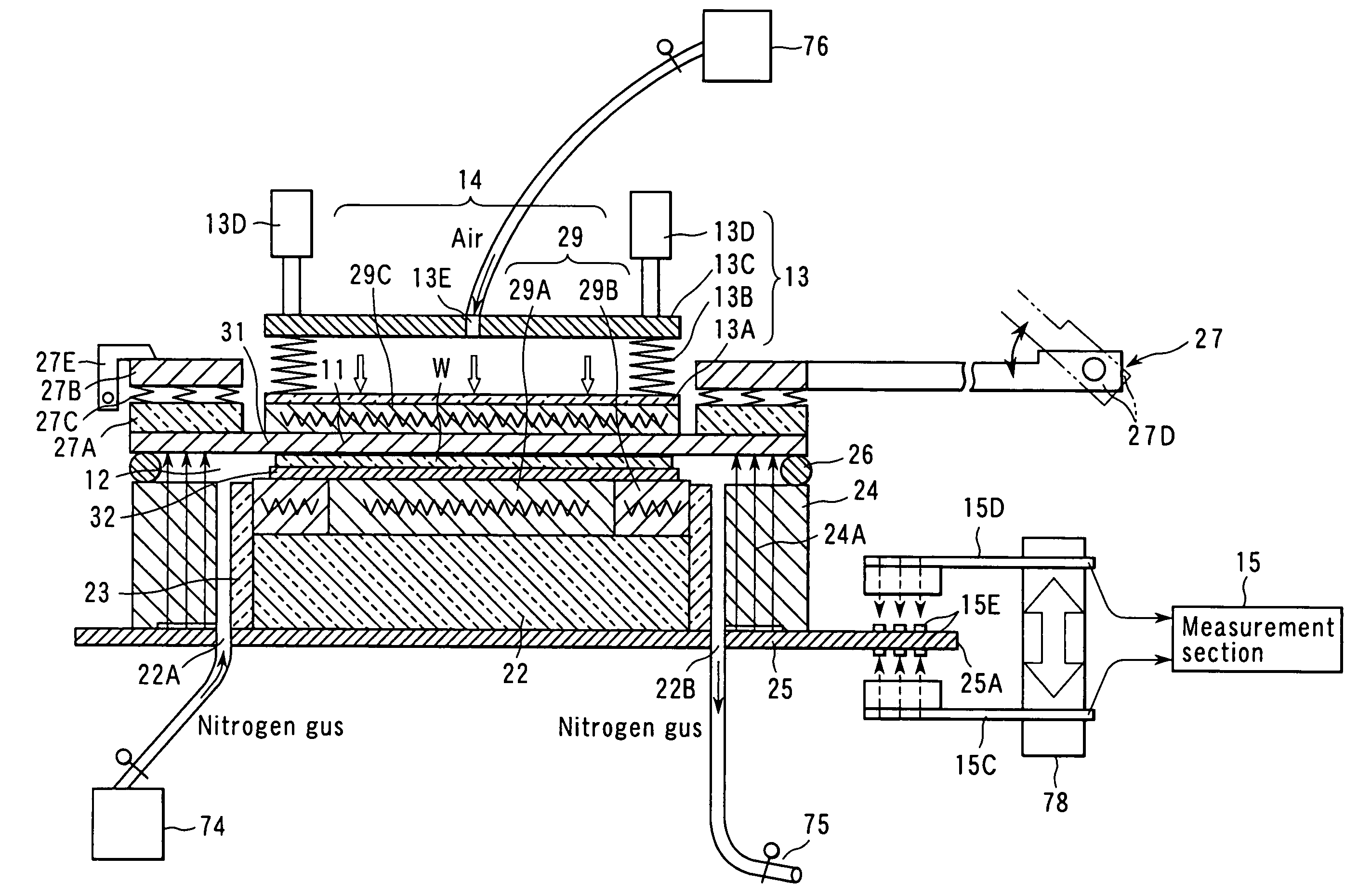
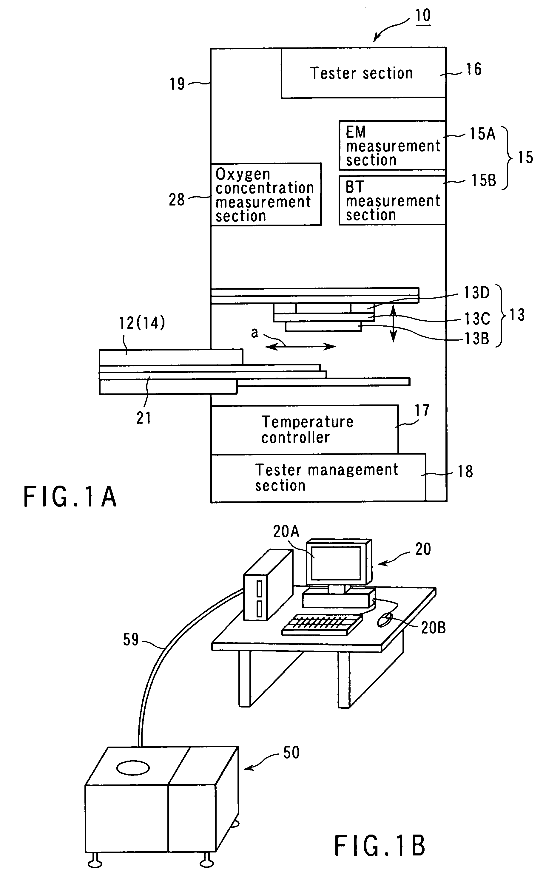
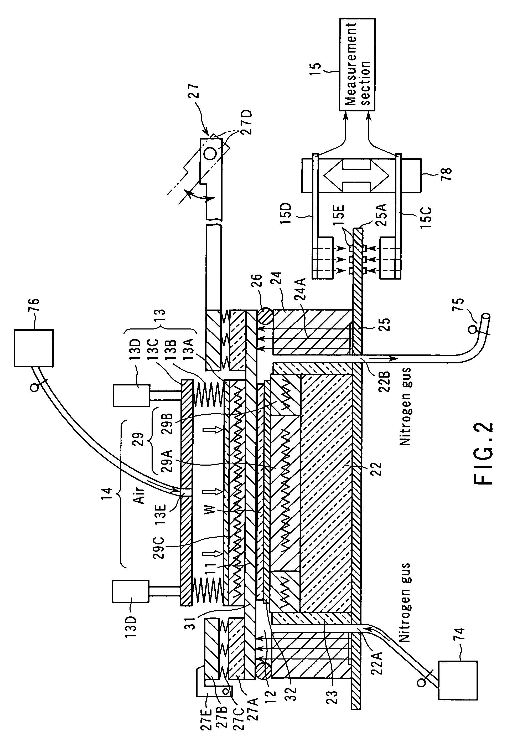
A reliability evaluation test apparatus of this invention includes a wafer storage section which stores a wafer in a state wherein the electrode pads of a number of devices formed on the wafer and the bumps of a contactor are totally in electrical contact with each other. The wafer storage section transmits / receives a test signal to / from a measurement section and has a hermetic and heat insulating structure. The wafer storage section has a pressure mechanism which presses the contactor and a heating mechanism which directly heats the wafer totally in contact with the contactor to a predetermined high temperature. The reliability of an interconnection film and insulating film formed on the semiconductor wafer are evaluated under an accelerated condition.

Description

CROSS-REFERENCE TO RELATED APPLICATIONS[0001]This is a Continuation Application of PCT Application No. PCT / JP02 / 12348, filed Nov. 27, 2002, which was not published under PCT Article 21(2) in English.[0002]This application is based upon and claims the benefit of priority from the prior Japanese Patent Application No. 2001-367268, filed Nov. 30, 2001, the entire contents of which are incorporated herein by reference.BACKGROUND OF THE INVENTION[0003]1. Field of the Invention[0004]The present invention relates to a reliability evaluation test apparatus, reliability evaluation test system, contactor, and reliability evaluation test method and, more particularly, to a reliability evaluation test apparatus, reliability evaluation test system, contactor, and reliability evaluation test method, which are used to evaluate / test the reliability of interconnections and insulating films which form multilayered interconnections for a number of semiconductor devices formed on a semiconductor wafer....

Claims


Application Information

Patent Timeline
Patent Type & Authority Patents(United States)
IPC IPC(8): G01R31/02G01R31/26G01R1/04G01R31/28G01R31/30H01L21/66
CPCG01R1/0433G01R1/0491G01R31/286G01R31/2865G01R31/2862G01R31/2831G01R31/2886G01R31/2867G01R31/287H01L22/00
Inventor TAKEKOSHI, KIYOSHIHOSAKA, HISATOMIHAGIHARA, JUNICHIHATSUSHIKA, KUNIHIKOUSUI, TAKAMASAKANEKO, HISASHIHAYASAKA, NOBUOIDO, YOSHIYUKI
Owner IBIDEN CO LTD
Learn More