Method for fabricating an interposer

a technology of interposers and components, applied in the field of interposers, can solve the problems of electrical shorts between adjacent bond wires, significant failure of semiconductor devices, and penetration of particulate die coats

Inactive Publication Date: 2006-08-22
MICRON TECH INC
View PDF69 Cites 50 Cited by
  • Summary
  • Abstract
  • Description
  • Claims
  • Application Information

AI Technical Summary

Benefits of technology

[0029]In stereolithographic processes, precise mechanical alignment of singulated interposers or larger substrates having multiple interposer locations is not required to practice the method of the present invention when machine vision is used to locate single substrates and features or other components thereon or associated therewith (such as bond pads, vias, solder bumps, etc.) or features on a larger substrate for alignment and material disposition purposes.

Problems solved by technology

However, it is now recognized that conventional packaging processes may cause significant numbers of semiconductor devices to fail.
For example, as a semiconductor device is being encapsulated, the protective material may cause particulate die coat penetration, “bond wire sweep,” which may break electrical connections made by the bond wires or cause electrical shorts between adjacent bond wires, and other problems.
Some state of the art semiconductor devices lack conventional packages (e.g., leads and encapsulants) or are minimally packaged.
When these types of semiconductor devices are tested, the solder bumps or other conductive structures protruding therefrom may not properly align with the corresponding test sockets of a test substrate so as to establish adequate electrical contacts between the tested semiconductor device and the test substrate.
Moreover, if misalignment occurs, the conductive structures may be damaged.
Nonetheless, the conductive structures protruding from a semiconductor device to be tested may be damaged when assembled with such an interposer.
Moreover, since the recesses of such interposers are configured to receive the conductive structures of a semiconductor device without stressing, deforming, or otherwise damaging the conductive structures, the interposer may fail to make adequate electrical connections between some of the conductive structures and their corresponding test pads or sockets of the test substrate.
Moreover, test interposers typically lack any alignment component other than the recesses thereof.
Accordingly, it appears that the art is lacking a structure for aligning the conductive structures of a semiconductor device with corresponding test pads or sockets of a test substrate without stressing or damaging the conductive structures while facilitating adequate electrical connections between the conductive structures and the test pads or sockets.
However, to the inventors' knowledge, stereolithography has yet to be applied to mass production of articles in volumes of thousands or millions, or employed to produce, augment or enhance products including other pre-existing components in large quantities, where minute component sizes are involved, and where extremely high resolution and a high degree of reproducibility of results are required.
Furthermore, conventional stereolithography apparatus and methods fail to address the difficulties of precisely locating and orienting a number of pre-existing components for stereolithographic application of material thereto without the use of mechanical alignment techniques or to otherwise assure precise, repeatable placement of components.
In particular, stereolithography has not been employed to fabricate interposers for aligning and connecting a semiconductor device to a test substrate.

Method used


Image

  • Method for fabricating an interposer
  • Method for fabricating an interposer
  • Method for fabricating an interposer

Examples


Embodiment Construction

The Interposer

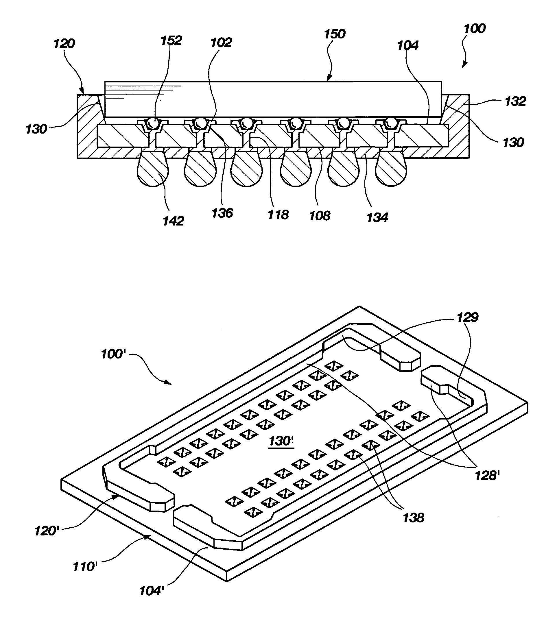
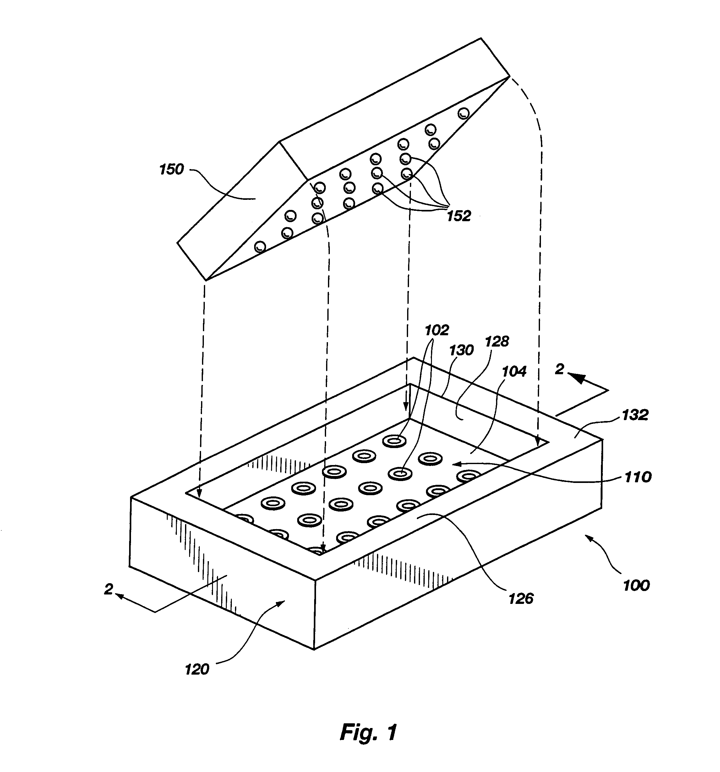
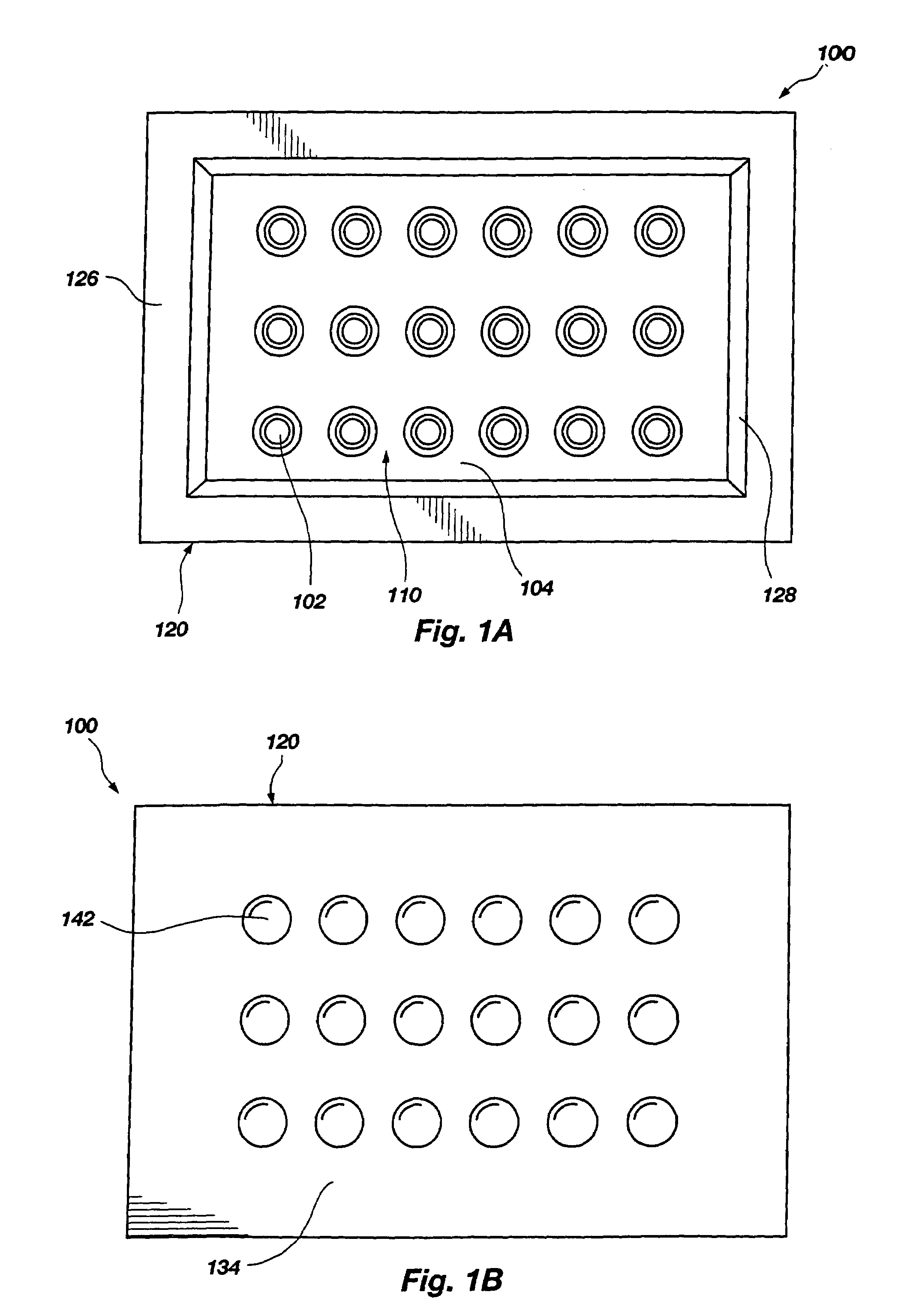
[0049]FIGS. 1, 1A, 1B, and 2 depict an exemplary interposer 100 of the present invention. Interposer 100 includes an interposer substrate 110 with contact pads 102 on a top surface 104 thereof and contact pads 106 on a bottom surface 108 thereof. Contact pads 102 may be recessed relative to top surface 104, as illustrated in FIG. 2. Contact pads 102 on top surface 104 of interposer substrate 110 communicate with corresponding contact pads 106 on bottom surface 108 by way of vias 118 filled or lined with metal 148 or another conductive material. Conductive structures 142, such as balls, bumps, or conductive pillars, of a conductive material, such as a solder, a metal, a metal alloy, a conductor-filled epoxy, a conductive epoxy, or a conductive (e.g., z-axis) elastomer, are secured to and protrude from contact pads 106 and from interposer 100.

[0050]Interposer substrate 110 may be fabricated from any suitable material for use in semiconductor device applications, such as ...


PUM

PropertyMeasurementUnit
thickaaaaaaaaaa
thicknessaaaaaaaaaa
sizeaaaaaaaaaa

Abstract

An interposer including a fence that receives and aligns a semiconductor device, such as a flip-chip type semiconductor device, with an interposer substrate. The fence may include edges that are configured to progressively align a semiconductor device with the interposer substrate. The fence may also include one or more laterally recessed regions to facilitate rough alignment of a semiconductor device with the interposer substrate. Methods for fabricating the fence include the use of stereolithographic and molding processes. When stereolithography is used to fabricate the fence, a machine vision system that includes at least one camera operably associated with a computer may be used to control a stereolithography apparatus and facilitates recognition of the position and orientation of interposer substrates on and around which material is to be applied in one or more layers to form the fence. As a result, the interposer substrates need not be precisely mechanically aligned.

Description

CROSS-REFERENCE TO RELATED APPLICATIONS[0001]This application is a continuation of application Ser. No. 09 / 843,119, filed Apr. 26, 2001, now U.S. Pat. No. 6,634,100, issued Oct. 21, 2003, which is a divisional of application Ser. No. 09 / 533,407, filed Mar. 23, 2000, now U.S. Pat. No. 6,529,027, issued Mar. 4, 2003.BACKGROUND OF THE INVENTION[0002]1. Field of the Invention[0003]The present invention relates generally to an interposer configured to receive a semiconductor device for testing. More specifically, the invention pertains to such a test interposer having an alignment fence for receiving and aligning semiconductor devices, such as flip-chip type semiconductor dice, ball grid array (BGA) packages, and chip scale packages (CSPs), with test sockets of the interposer. The present invention also relates to methods for fabricating such a test interposer.[0004]2. Background of Related Art[0005]The semiconductor industry produces extremely large numbers of miniature electrical devic...

Claims


Application Information

Patent Timeline
Patent Type & Authority Patents(United States)
IPC IPC(8): H01R43/16G01R1/04H05K1/11H05K1/14H05K3/34
CPCG01R1/0408G01R1/0466G01R1/0483G01R1/07378H01L23/32H01L23/49827H01L24/72H05K1/141H05K7/1061G01R1/0433Y10T29/4913G01R3/00H01L2224/16H01L2924/01049H01L2924/01082H01L2924/12044H05K1/112H05K3/3436H05K2201/049H05K2201/09472H05K2201/10378H05K2201/10734H05K2201/2018H05K2203/167H01L2924/01005H01L2924/01006H01L2924/01033H01L2224/16225H01L2224/16237H01L2224/8114Y10T29/49144Y10T29/49156Y10T29/49218Y10T29/49165Y10T29/49126Y10T29/49147Y10T29/49222Y10T29/49204B33Y10/00B33Y30/00B33Y80/00H01L2224/16111H01L2224/81385H01L2924/12042H01L2924/15787H01L2924/351H01L2924/00
Inventor AKRAM, SALMANWOOD, ALAN G.FARNWORTH, WARREN M.
Owner MICRON TECH INC
Why Eureka
Try Eureka