High performance MIS capacitor with HfO2 dielectric

a dielectric capacitor and high-performance technology, applied in semiconductor devices, chemical vapor deposition coatings, coatings, etc., can solve the problems of significant technical barriers to the successful production of such materials, limiting the capacitance, and increasing the problem of step coverage and loading effects

a dielectric capacitor and high-performance technology, applied in semiconductor devices, chemical vapor deposition coatings, coatings, etc., can solve the problems of significant technical barriers to the successful production of such materials, limiting the capacitance, and increasing the problem of step coverage and loading effects

US7094712B2Inactive Publication Date: 2006-08-22SAMSUNG ELECTRONICS CO LTD

Image

  • High performance MIS capacitor with HfO2 dielectric
  • High performance MIS capacitor with HfO2 dielectric
  • High performance MIS capacitor with HfO2 dielectric

Examples


Embodiment Construction

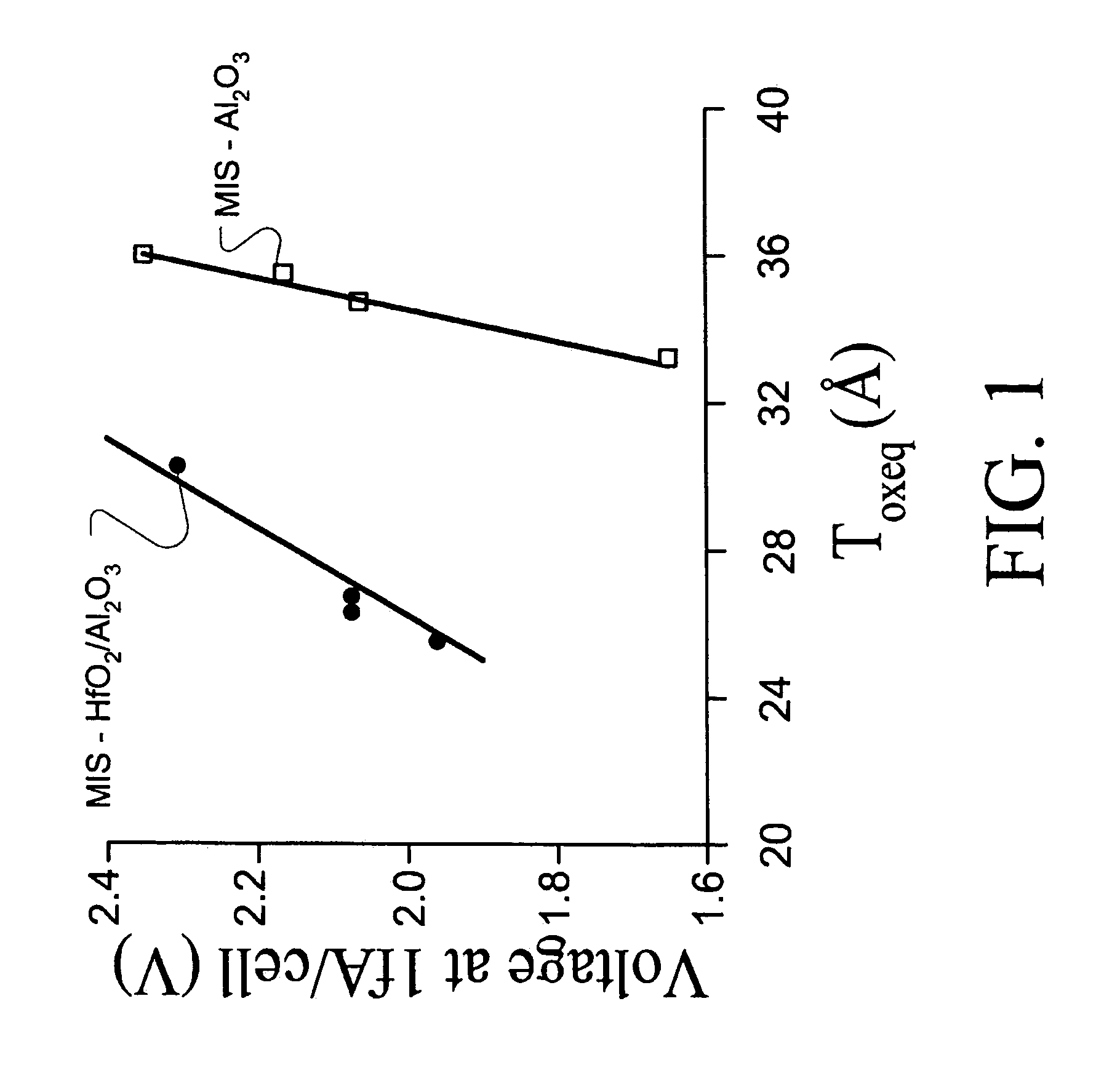
[0038]Hafnium oxide, HfO2, has been identified as a promising dielectric material when used either singly or in combination with other insulating materials such as alumina Al2O3. A combination of HfO2 and Al2O3, when used as the dielectric layer in a metal-insulator-silicon (MIS) capacitor produces a lower Toxeq than a MIS capacitor using a single Al2O3 film. As reflected in FIG. 1, the combination of HfO2 and Al2O3 as the dielectric film in a MIS capacitor shows improved scaling characteristics compared with the use of Al2O3 alone.

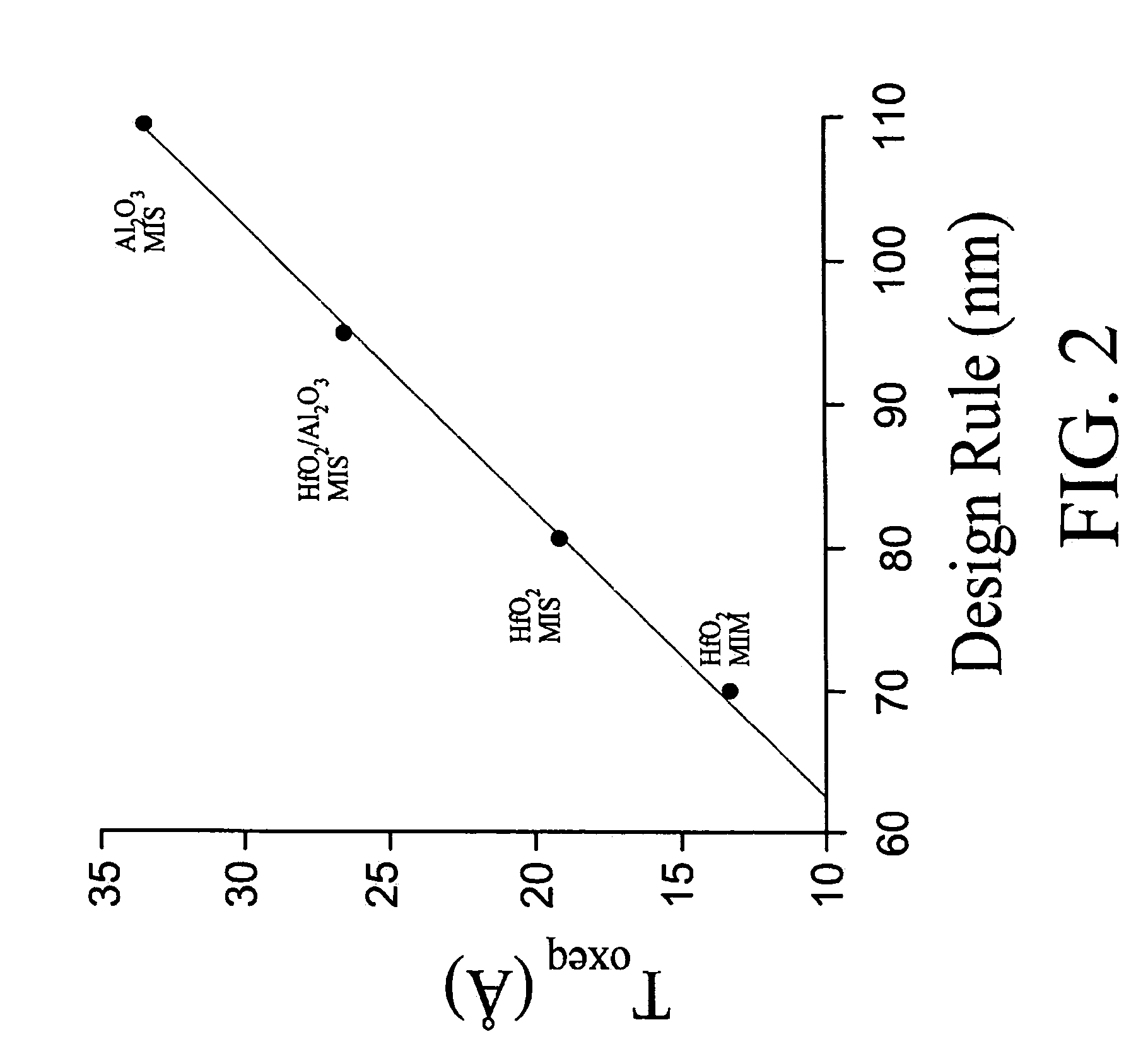
[0039]As reflected in FIG. 2, for devices built to design rules below about 110 nm, Al2O3 should be replaced by a combination of HfO2 and Al2O3. As also reflected in FIG. 2, for devices built to design rules below about 90 nm, the combination of HfO2 and Al2O3 should, in turn, be replaced by a HfO2 film in either a MIS or a metal-insulator-metal (MIM) configuration to obtain even lower Toxeq values.

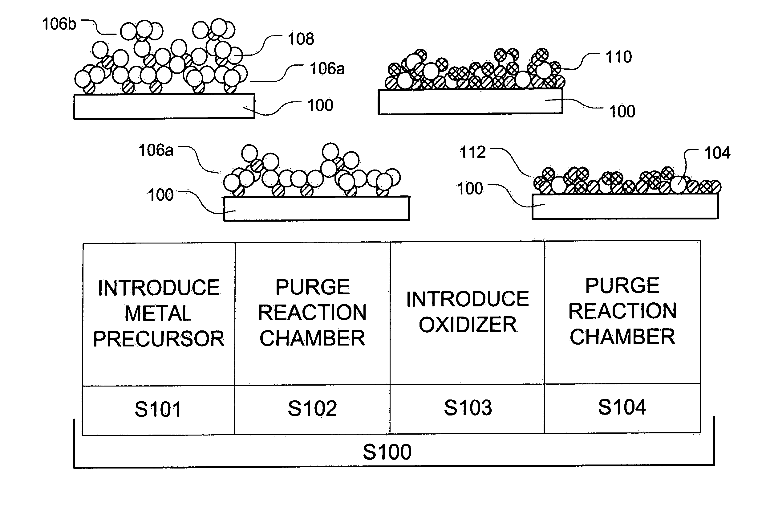
[0040]A single HfO2 layer, however, may be subject to deg...


PUM

PropertyMeasurementUnit
temperatureaaaaaaaaaa
pressureaaaaaaaaaa
temperatureaaaaaaaaaa

Abstract

Disclosed is a method for forming metal oxide dielectric layers, more particularly HfO2 dielectric layers, using an atomic layer deposition (ALD) method in which a series of thin intermediate layers are formed and treated with one or more oxidizers and nitrogents before the next intermediate layer is formed on the substrate. The intermediate oxidation treatments reduce the number of organic contaminants incorporated into the metal oxide layer from the organometallic precursors to produce a dielectric layer having improved current leakage characteristics. The dielectric layers formed in this manner remain susceptible to crystallization if exposed to temperatures much above 550° C., so subsequent semiconductor manufacturing processes should be modified or eliminated to avoid such temperatures or limit the duration at such temperatures to maintain the performance of the dielectric materials.

Description

CROSS-REFERENCE TO RELATED CASES[0001]This U.S. nonprovisional patent application claims priority under 35 U.S.C. § 119 of Korean Patent Application 2003-67809 filed on Sep. 30, 2003 and Korean Patent Application 2004-11765 filed on Feb. 23, 2004, the entire contents of which are hereby incorporated by reference.BACKGROUND OF THE INVENTION[0002]1. Field of the Invention[0003]The present invention relates to an improved method for manufacturing semiconductor devices, and more particularly, to an improved atomic layer deposition (ALD) method for forming thin, high-quality HfO2 layers suitable for use as a dielectric material in such semiconductor devices.[0004]2. Description of the Related Art[0005]As the scale of semiconductor devices has decreased, the need for ultra-thin layers has gradually increased. However, the formation of ever thinner layers necessitates other process adjustments such as lower thermal budgets and the use of new materials. In addition to the thermal budget con...

Claims


Application Information

Patent Timeline
22 Aug 2006
Publication
US7094712B2
IPC
H01L21/31; C23C16/40; C23C16/455; H01L21/28; H01L21/314; H01L21/316; H01L29/49; H01L29/51; H10B12/00
CPC
C23C16/405; C23C16/45529; C23C16/45531; H01L21/28088; H01L21/28185; H01L21/3141; H01L21/31645; H01L29/4966
Inventors
IM, KI-VIN; PARK, KI-YEON