

Laser annealing apparatus
a technology of lattice defects and heat treatment equipment, which is applied in the direction of chemistry apparatus and processes, crystal growth process, polycrystalline material growth, etc., can solve the problems of low efficiency of thin film transistors, low productivity, and difficulty in fabricating integrated circuits requiring high speed and high functionality, and achieve high productivity of silicon thin films, small lattice defects density, and high crystallinity
- Summary
- Abstract
- Description
- Claims
- Application Information
AI Technical Summary
Benefits of technology
Problems solved by technology
Method used
Image

Examples
embodiment 1
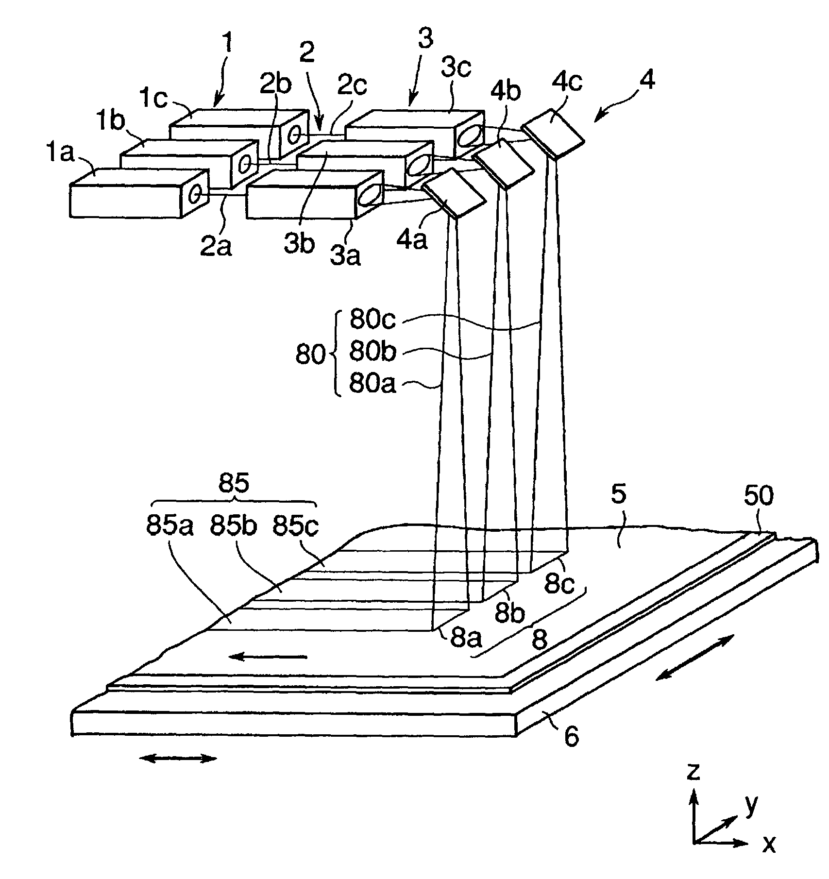
[0026]A laser annealing apparatus of this embodiment comprises three laser oscillators 1a to 1c, and three laser optical systems having the linear beam forming means 3a to 3c and the reflecting mirrors 4a to 4c that are arranged so that the beam optical axes may be substantially horizontal, the reflecting mirrors 4a to 4c being disposed above a substrate 50 on a stage 6, as shown in FIG. 1.
[0027]The laser beams 2 (2a to 2c) are radiated from three laser oscillators 1 (1a to 1c) toward the linear beam forming means 3 (3a to 3c) as the corresponding laser optical systems, and each of the linear beam forming means 3a to 3c forms the laser beam to have a linear profile of beam on the silicon film. The beams from the linear beam forming means 3 (3a to 3c) are reflected from the reflecting mirrors 4 (4a to 4c), respectively, and applied vertically on the surface of the silicon film 5.
[0028]Each of the linear beam forming means 3 forms the laser beam 2 so that radiating laser beam 8a, 8b a...
embodiment 2
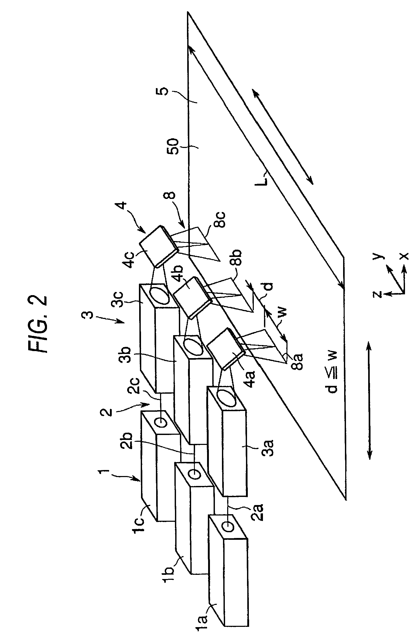
[0044]FIG. 2 is a typical perspective view of an optical system for the laser annealing apparatus according to an embodiment 2 of this invention. In this embodiment 2, the radiating laser beam interval d is set to be equal to or slightly smaller than the radiating laser beam width w. In addition, the structure of the laser optical system and the action and function of radiating laser beams on the amorphous or polycrystalline silicon film are the same as described in the embodiment 1.
[0045]With this arrangement of radiating laser beams, after the first scanning pass, the amount of movement of the silicon film in the y direction is made almost equal to the radiating laser beam interval d, whereby the laser beams can be applied on the substrate over the area width L required for laser radiation, resulting in the even heat treatment.
embodiment 3
[0046]In this embodiment 3, the interval d between the linearly radiating laser beams is set to meet the relation
(w+d)×n≧L
where w is the laser beam width, d is the laser beam interval, L is the area width for laser radiation on the substrate, and n is the number of laser beams, as shown in FIG. 3. In this embodiment 3, the structure of the laser optical system and the action and function of radiating laser beams on the amorphous or polycrystalline silicon film are also the same as described in the embodiment 1.
[0047]With the above array of radiating laser beams, the spacing between laser optical systems for the plural laser beams can be maximized, whereby the plurality of laser optical systems including the linear beam forming means can be arranged with distance, thereby preventing interference between optical parts. The amount of movement for the substrate 50 in the y direction through one pass can be reduced to them in minimum interval, thereby stabilizing the operation of a movem...
PUM
 Abstract
Description
Claims
Application Information