Large modal volume semiconductor laser system with spatial mode filter

a semiconductor laser and spatial mode technology, applied in semiconductor lasers, laser optical resonator construction, laser details, etc., can solve the problems of single spatial mode design dilemma, achieve a larger mode size in a waveguide that supports only a lowest-order, etc., and achieve larger mode sizes and shapes. , the effect of reducing the numerical aperture of the output beam

Inactive Publication Date: 2006-09-12
WALPOLE JAMES N +1
View PDF14 Cites 3 Cited by
  • Summary
  • Abstract
  • Description
  • Claims
  • Application Information

AI Technical Summary

Benefits of technology

[0003]For many applications, it would be useful if the dimensions of the mode could be made larger in both the lateral and transverse directions, and particularly in the transverse direction. Larger dimensions would lead to a reduction in the numerical aperture of the output beam, and the beam could be more nearly round, rather than being elliptical in cross-section with a large aspect ratio of the major to minor axes. These larger mode sizes and shapes would be especially attractive when the optical output of the semiconductor device is to be coupled into a single-mode optical fiber.

Problems solved by technology

Fundamentally, the achievement of a larger mode size in a waveguide that supports only a lowest-order, single spatial mode is a design dilemma.

Method used


Image

  • Large modal volume semiconductor laser system with spatial mode filter
  • Large modal volume semiconductor laser system with spatial mode filter
  • Large modal volume semiconductor laser system with spatial mode filter

Examples


Embodiment Construction

[0024]This teaching of U.S. provisional patent application No. 60 / 263,683, filed Jan. 23, 2001, are hereby incorporated by this reference.

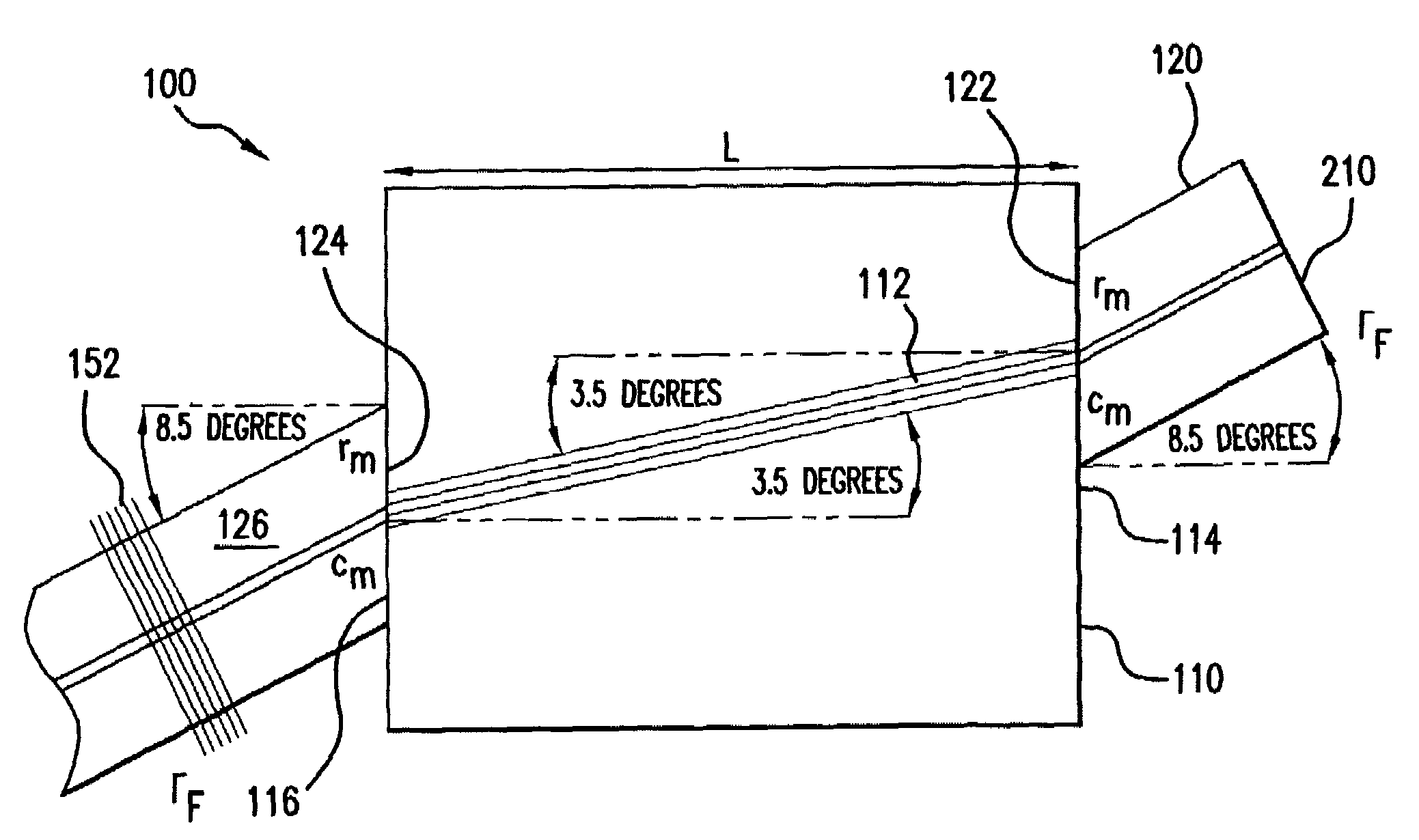
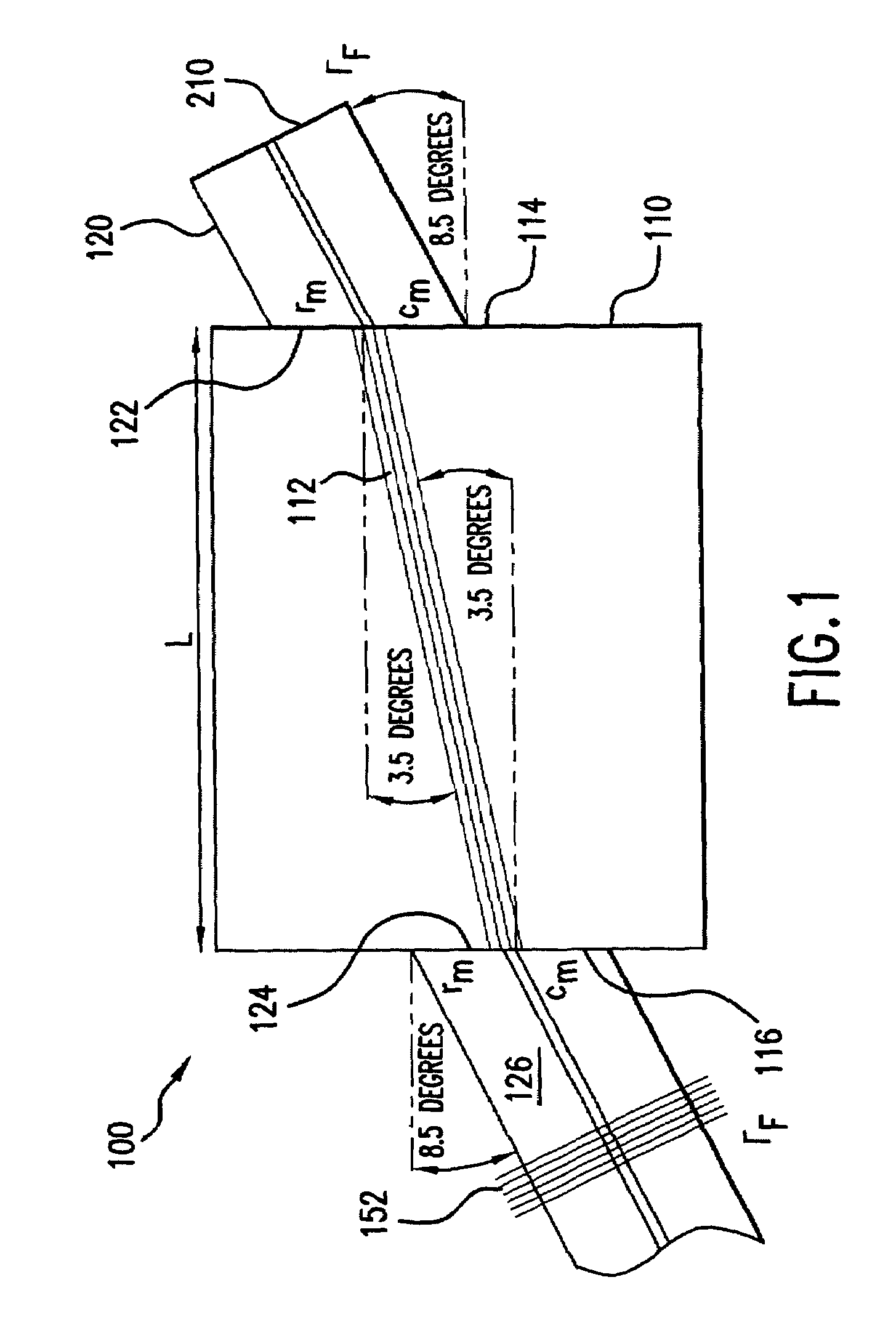
[0025]FIG. 1 shows an external cavity semiconductor laser system 100, which has been constructed according to the principles of the present invention.

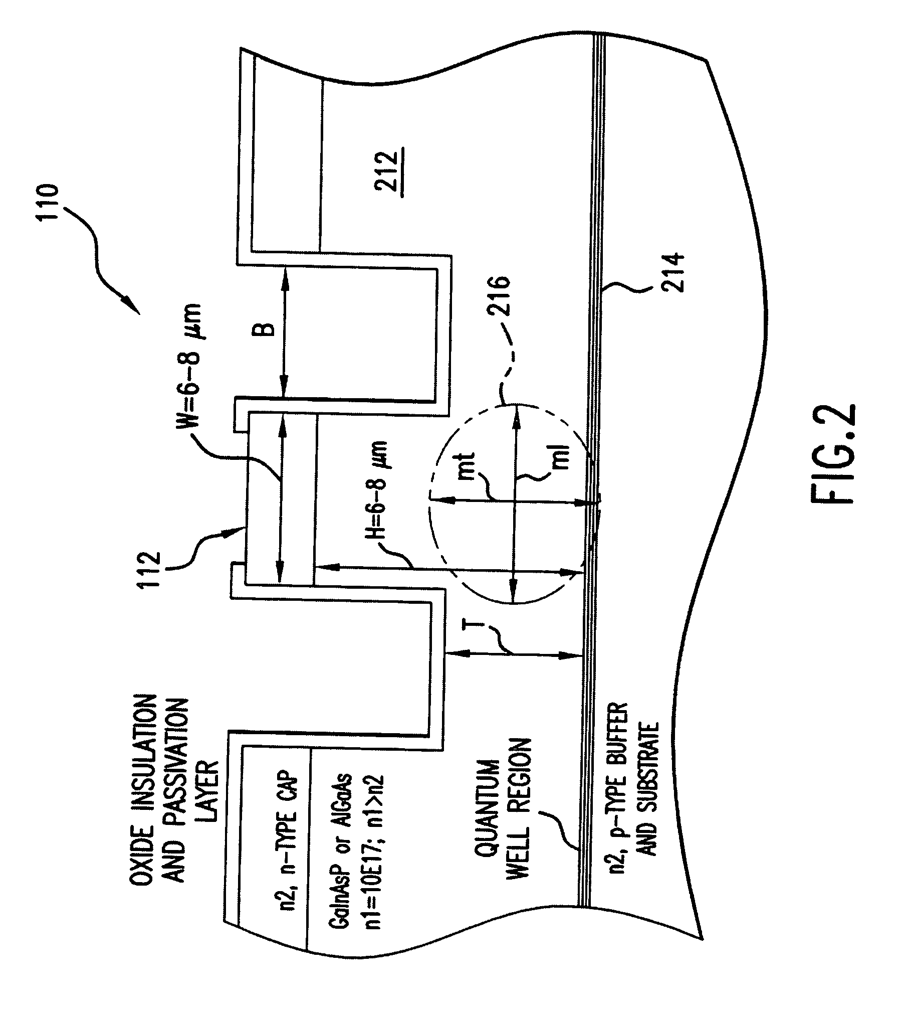
[0026]Generally, the laser 100 comprises a semiconductor chip 110. This chip has a stripe 112, such as a ridge waveguide, which has been etched or otherwise formed in the epitaxial layers of the bulk material of the chip 110. The stripe 112 defines the optical axis.

[0027]In one implementation, the chip utilizes a trench-defined ridge. In alternative embodiments, the epitaxial layers on either lateral side of the ridge are entirely removed as in another common ridge configuration. In still other embodiments, stripes defined by regrowth or other processes are used.

[0028]According to the invention, the chip 110 is configured to generate a mode that is greater than 5 micrometers in diameter in both the t...


PUM


Abstract

A semiconductor optical amplification system that uses a single-mode fiber angle-coupled to a semiconductor wave-guide medium with optical gain. This design is particularly simple and relevant to optical fiber systems, but it may be generalized to include other implementations as well, in which other spatial mode filters are employed. A chip design is employed in which lowest order mode has a size greater than about 5 micrometers (μm). Thus, much smaller facet angles can be employed while still avoiding self-oscillation. More specifically, according to some aspects of the invention, facet angles of less than 4 to 5 degrees are utilized.

Description

RELATED APPLICATIONS[0001]This application is a Continuation of U.S. application Ser. No. 10 / 055,872 filed on Jan. 23, 2002 now U.S. Pat. No. 6,804,281 which claims benefit of provisional application No. 60 / 263,683 filed on Jan. 23, 2001, both of which are incorporated herein by reference in their entirety.BACKGROUND OF THE INVENTION[0002]Conventional edge-emitting semiconductor devices such as lasers and semiconductor optical amplifiers (SOA's) usually comprise a substrate, on which epitaxial layers of varying alloy compositions, carrier types and carrier densities have grown. These various layers are used to define the optical waveguide and the gain region of the device, which are designed to support amplification and emission of radiation in a single spatial mode. Typically, for high power devices, the dimensions of the cross-sectional area of the single spatial mode are a few micrometers in the direction parallel to the epitaxial layers (the lateral direction) and a fraction of ...

Claims


Application Information

Patent Timeline
Patent Type & Authority Patents(United States)
IPC IPC(8): H01S5/00H01S5/10H01S5/14
CPCH01S5/10H01S5/146H01S5/1085
Inventor WALPOLE, JAMES N.NILL, KENNETH W.
Owner WALPOLE JAMES N
Why Eureka
Try Eureka