Capping layer for reducing amorphous carbon contamination of photoresist in semiconductor device manufacture; and process for making same

Active Publication Date: 2006-09-19
NXP USA INC
View PDF21 Cites 27 Cited by
  • Summary
  • Abstract
  • Description
  • Claims
  • Application Information

AI Technical Summary

Benefits of technology

[0012]The optical properties of primary interest to impart to the capping stack are: refractive index, denoted hereinafter “n”; and extinction coefficient, hereinafter “k”. The complex refractive index is ñ=n+ik according to standard definitions. For optimal stacking layers according to the invention, these values will vary depending on the photolithographic wavelength used on the resist, on the materials chosen for the capping stack, and on the material thicknesses. In general, the optical properties of the capping layer are selected to minimize the overall reflectivity of the stack.
[0013]A capping stack for an amorphous carbon layer is realized in one embodiment by combining an SiON layer with one or more additional layers of a silicon-rich oxide. The desired thicknesses of the capping layer materials a

Problems solved by technology

The neutralization results in a failure to remove the resist in the desired region during the develop step which uses mild basic chemistry, thereby leading to the formation of a region of undesired resist—also known as an “extra pattern” of resist.
Extra resist patterns are defects since the pattern on the photolithographic mask is not transferred to the wafer with perfect fidelity.
The extra resist patterns can distort the shape of printed features, which can affect conductivity and adversely impact the feature's influence on underlying layers, as by affecting channel length, for example.
If the extra patterns are sufficiently large—in the vicinity

Method used


Image

  • Capping layer for reducing amorphous carbon contamination of photoresist in semiconductor device manufacture; and process for making same
  • Capping layer for reducing amorphous carbon contamination of photoresist in semiconductor device manufacture; and process for making same

Examples


Example

Example 1

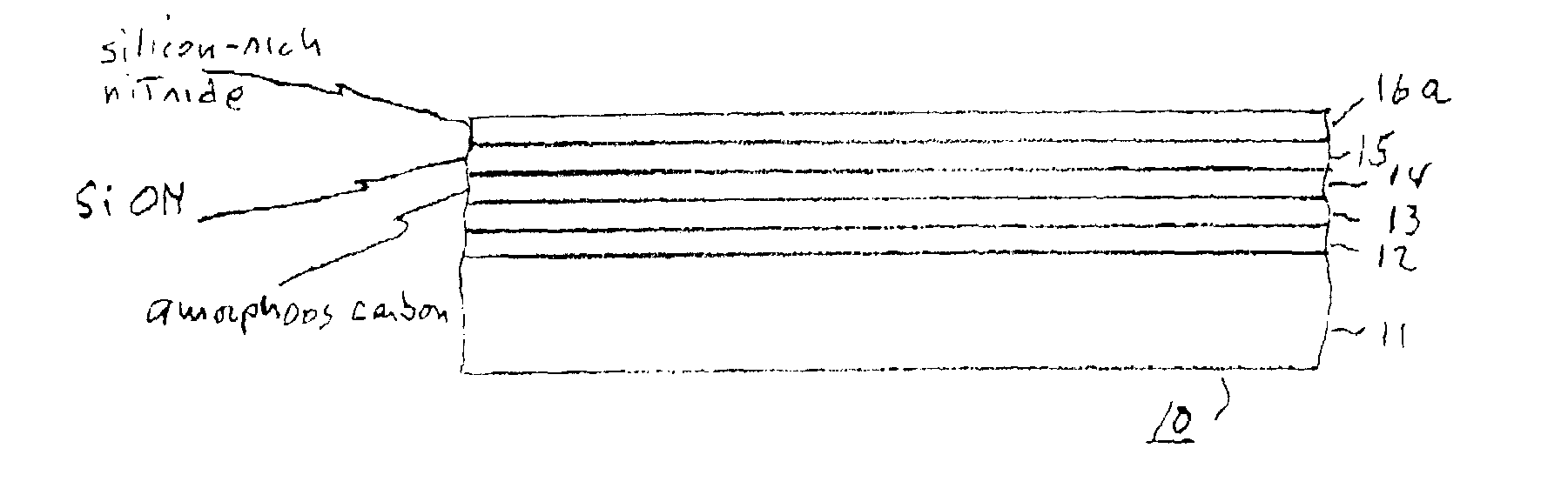
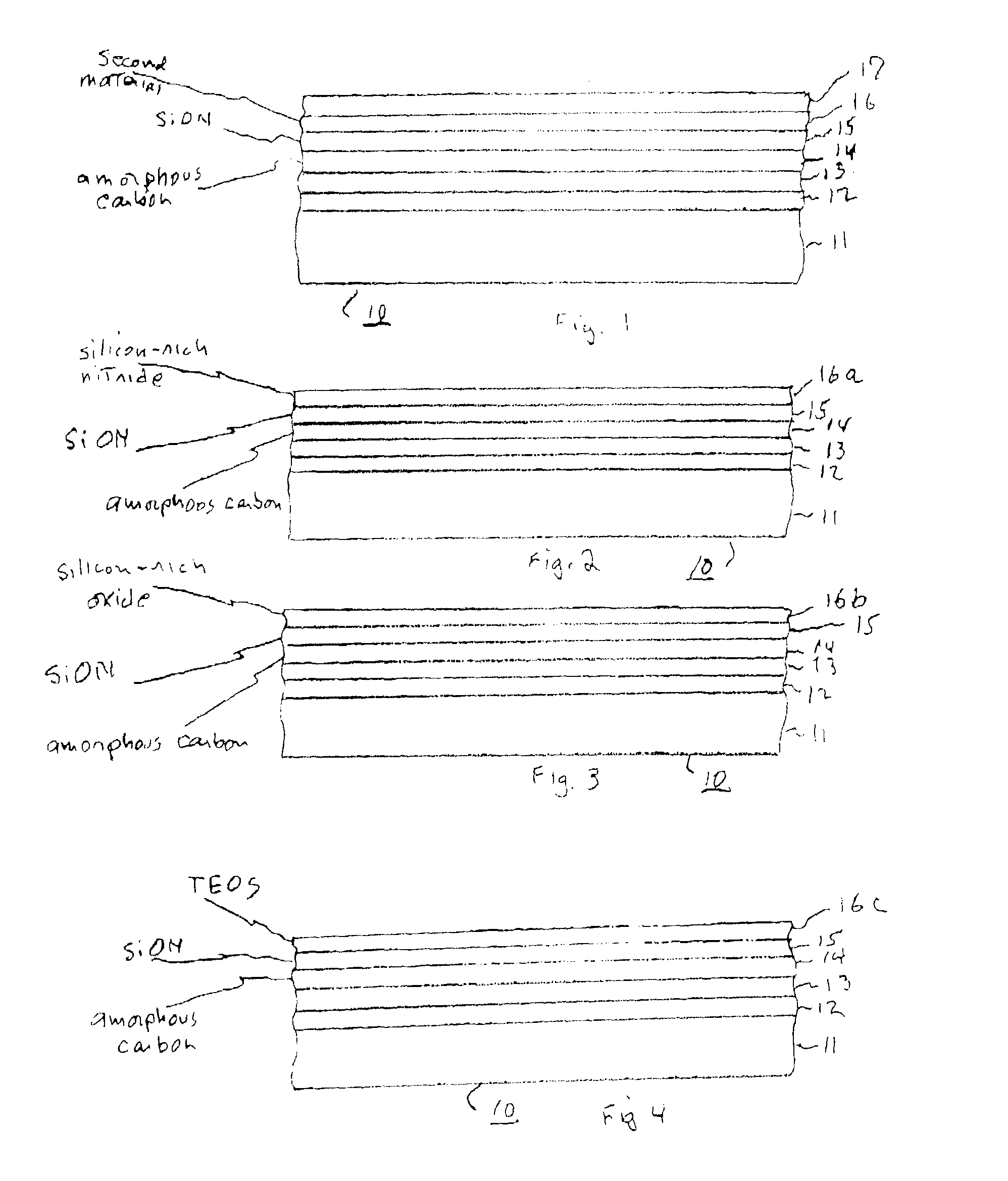
[0023]In FIG. 2, a capping stack buildup consisting of SiON layer 15 and a second material comprising silicon-rich nitride layer 16a is formed on top of amorphous carbon layer 14. The SiON may be placed either on top of the silicon-rich nitride layer 16a or below it. Deposition of SiON is effected by flowing 3–6 liter / min N2, 100–300 sccm SiH4 gas, and 50–300 sccm N2O gas. The plasma is maintained at 350–500 degrees C. and at 3–8 Torr pressure. RF plasma power is maintained at between 250 and 500 Watts. With these conditions, typical deposition rates of SiON are 30–150 A / sec. These process parameters may be varied to achieve the desired control over the deposition thickness and optical properties. Specifically, the layer 15 of SiON suitable for 193 nm photoresist system is 200 nm in thickness and with optical values n=1.8±0.10 and k=0.3±0.05. These values are optimal because of the resulting low reflectivity leading to minimal CD swing and thereby better CD control and unif...

Example

Example 2

[0024]In FIG. 3, a capping stack buildup consisting of SiON layer 15 and a second material comprising silicon-rich oxide layer 16b is formed on top of amorphous carbon layer 14. The SiON is deposited as in Example 1. To deposit silicon-rich oxide, SiH4 gas is flowed at 50–300 sccm, N2 gas is flowed at 1–2 liter / minute, and N2O gas is flowed at 100 cc–7 liters / minute. Pressure of 800 mT to 3 Torr, wafer temperature of 350–500 degrees C., and plasma power between 250–600 watts are maintained. As in Example 1 process parameters are varied to achieve desired control over the deposition thickness and optical properties. Thus layer 16b of silicon-rich oxide film suitable for the reflectivity requirements of a 193 nm photoresist process, is approximately 200 Angstroms thick, although thickness can vary between about 50 to 200 Angstroms. Layer 16b is produced with optical values of n=1.75±0.10 and k=0.2±0.2v. These are optimal because of the resulting low reflectivity leading to sm...

Example

Example 3

[0025]In FIG. 4, a capping stack buildup is realized consisting of an SiON 15 and a second material comprising TEOS oxide layer 16c (oxide deposited using Tetra Ethyl Ortho Silicate precursor). The SiON is deposited as in Example 1. Then, either above or below the SiON layer 15, the layer 16c of TEOS oxide is deposited. The deposition of TEOS oxide in the PECVD process is conventional using well-known TEOS precursors. Again, process parameters are varied to achieve desired control over the deposition thickness and optical properties. A layer of TEOS oxide film suitable for the 193 nm photoresist process is approximately 250 Angstroms thick, but may vary in thickness from about 150 to 300 Angstroms; and has values of n=1.67±0.07 and k=0.1±0.1v.

[0026]In summary, the capping stacks exemplified above enable the requisite low reflectance to be obtained in the layers below the photoresist, while keeping the amorphous carbon and the photoresist separated more effectively through t...


PUM


Abstract

In the fabrication of semiconductor devices using the PECVD process to deposit hardmask material such as amorphous carbon, structure and process are described for reducing migration of species from the amorphous carbon which can damage an overlying photoresist. In one embodiment useful to 248 nm and 193 nm photolithography exposure wavelengths, amorphous carbon is plasma-deposited on a substrate to pre-defined thickness and pre-defined optical properties. A SiON layer is combined with a silicon-rich oxide layer, a silicon-rich nitride layer or a TEOS layer to create a capping layer resistant to species-migration. Layers are formulated to pre-determined thicknesses, refractive indices and extinction coefficients. The capping stacks constitute an effective etch mask for the amorphous carbon; and the hardmask properties of the amorphous carbon are not compromised. The disclosure has immediate application to fabricating polysilicon gates.

Description

TECHNICAL FIELD[0001]This invention relates to use of photoresist films in semiconductor device manufacturing; and more particularly to materials and processes for avoiding migration of species between the film and an amorphous carbon layer in the device.BACKGROUND OF THE INVENTION[0002]In the build-up of layers of a semiconductor device, features are lithographically defined by placing photoresist onto an underlying layer and selectively exposing the resist to a pre-selected wavelength of light. The exposure causes a photo-sensitive chemical reaction to occur in the photoresist, which creates patterns that determine features in underlying layers. Thereafter, the photoresist is developed, which removes unwanted areas and creates a desired feature pattern for the underlying layer. The patterned photoresist is then used as an etch mask to transfer the pattern into the underlying layer; or onto a hardmask atop the underlying layer that performs the pattern transfer.[0003]The photoresis...

Claims


Application Information

Patent Timeline
IPC IPC(8): H01L21/3205H01L21/4763H01L23/58H01L29/76H01L29/788
CPCH01L21/0332H01L21/32139H01L21/28044H01L2924/0002H01L2924/00
Inventor WRIGHT, MARILYN I.DAKSHINA-MURTHY, SRIKANTESWARAJUNKER, KURT H.PATTERSON, KYLE
Owner NXP USA INC
Why Eureka
Try Eureka