Electronic element operable at room temperature using super-dielectric phenomenon

a super-dielectric phenomenon and electric element technology, applied in the field of electric element, can solve the problems of not much faster than a semiconductor element, and its performance is also inferior to that of a semiconductor element, and achieve the effect of eliminating unwanted external fields and facilitating observation

Inactive Publication Date: 2006-09-19
YOKOHAMA TLO
View PDF0 Cites 3 Cited by
  • Summary
  • Abstract
  • Description
  • Claims
  • Application Information

AI Technical Summary

Benefits of technology

[0049]In the following examples, to facilitate observation, “an initialization step” is performed on thin film of thin plate (001) crystal of a perovskite crystal insulator / conductor, wherein (i) a special sample structure is sandwiched between the metal plates, and (ii) charge and magnetic flux trapped before measurement, is eliminated by heating, etc., and a sufficient electric field / magnetic field shielding is used during measurements to eliminate unwanted external fields.

Problems solved by technology

However, as this element uses a superconductor, a low temperature environment such as liquid helium temperature or liquid nitrogen temperature is required, and as it has an operational limiting frequency of 1 THz, it is not much faster than a semiconductor element.
In addition, the usual electrodes and wires cannot be attached, and as it has an operational limiting frequency of about 1GHz, its performance is also inferior to that of a semiconductor element.

Method used


Image

  • Electronic element operable at room temperature using super-dielectric phenomenon
  • Electronic element operable at room temperature using super-dielectric phenomenon
  • Electronic element operable at room temperature using super-dielectric phenomenon

Examples


example 1

Relation Between Fractional Quantum Hall Effect and Super Dielectric Effect of Electronic Element

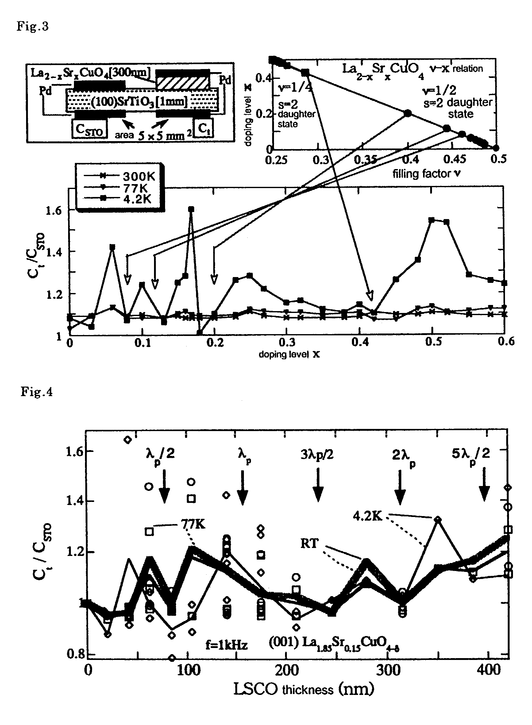
[0050]An electronic element having the sample shape in the upper left part of FIG. 3 was manufactured according to the following procedure. A 50 nanometer Pd thin film was grown by vacuum vapour deposition without substrate heating parallel to the (100) plane on both surfaces of a Furuuchi Chemicals (100) SrTiO3 single crystal double-surface optically polished substrate (surface area 10×20 mm2, thickness 1 mm), and shaped by dry etching to form an electrostatic capacitance structure known as a Pd / (100)SrTiO3 / Pd CSTO of surface area 5×5 mm2. Also, a La2−xSrxCuO4 thin film was grown in part of the same substrate using a high frequency magnetron sputtering apparatus from a solid target of La2−xSrxCuO4 at a substrate temperature of 700° C. at an input power of 70W in a Ar / O2 gas mixture at 8 Pa, such that its (100) plane (xy plane, i.e. two-dimensional plane) was parallel to the aforesaid (1...

example 2

Relation Between Film Thickness and Super Dielectric Effect of Electronic Element

[0061]An electronic element was manufactured in an identical way to that of Example 1, except that the surface area of the electrostatic capacitance structure was 7 mm2, and the doping amount was 0.15.

[0062]A test was performed in an identical way to that of Example 1, using an identical measurement instrument to that of Example 1, at a frequency of 1 KHz, voltage of 1Vpp and temperatures of room temperature, 77K and 4.2K. The results are shown in FIG. 4. The broken line is the average value of the measurement values for each temperature and film thickness.

[0063]As can be seen from FIG. 4, Ct / CSTO decreases when the film thickness of a

[0064]La2−xSrxCuO4−σ thin film is a specific value. Regarding the film thickness when there is a decrease, if the plasma oscillation wavelength of Equation (1) is calculated for La2−xSrxCuO4, λp is approximately 150 nm. Using this result, the film thickness when Ct / CSTO de...

example 3

Single Charge Interference Due to Quantum Resonance with Laser Light

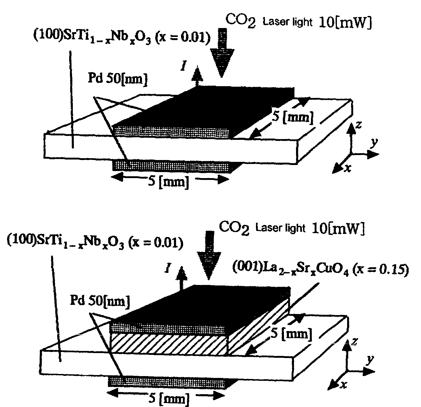
[0065]The form of the electronic element used for laser light and quantum resonance is shown in FIG. 5. In the electronic element in the upper part of FIG. 5, the (100) plane (i.e., two-dimensional plane) of SrTi1−xNbxO3 crystal was disposed parallel to a Pd film, and its thickness was 1 mm. On the other hand, in the electronic element in the lower part of FIG. 5, a La2−xSrxCuO4−σ film was added to the electronic element in the upper part of FIG. 5, the (001) plane (i.e., two-dimensional plane) of La2−xSrxCuO4−σ film crystal was disposed parallel to the (100) plane of the aforesaid SrTi1−xNbxO3 crystal and the Pd film, and its thickness was 100 nm. During manufacture, it is important that the crystal surface (end region) part which directly connects the electrodes has a good surface state, so the La2−xSrxCuO4−σ thin film was manufactured by the laser vapor deposition method which makes it relatively easy to obtain g...


PUM


Abstract

This invention relates to an electronic element having an electron function which acts even at room temperature using a super dielectric effect. The element has a crystalline electron system, and uses a perovskite crystal in the ground state of a “macroscopic quantum effect” which occurs when the electron number is defined, or nearly defined. The electronic element used in an electric field such that the two-dimensional plane of doped crystals ground state of a “fractional quantum Hall effect” wherein the doping amount of the crystals is 0.05 or less, or if localization is introduced, 0.6 or less, and the crystals may have a doping amount variation determined by the degree of localization.

Description

FIELD OF THE INVENTION[0001]This invention relates to an electronic element having an electron function which acts even at room temperature using a super dielectric effect. The element has a crystalline electron system, and uses a perovskite crystal in the ground state of a macroscopic quantum effect which occurs when the electron number is defined, or nearly defined (an effect shown by samples of macroscopic dimensions of the order of mm and cm wherein a large number of particles behave like a single particle). This “super dielectric effect” is a dual effect (a property wherein magnetic flux and current, etc., correspond to charge and field) of superconductivity which is a “macroscopic quantum effect” with a defined phase. The characteristics of the superconductor are as follows.[0002](i) The magnetic flux penetrating the “superconductor” tends to be expelled. (ii) The relation between the vector potential A and current density j is such that j / A is negative. (iii) The magnetic flu...

Claims


Application Information

Patent Timeline
Patent Type & Authority Patents(United States)
IPC IPC(8): H01L29/06H01L49/00
CPCH01L49/006H10N99/05
Inventor SUGAWARA, MASANORI
Owner YOKOHAMA TLO
Why Eureka
Try Eureka