

Bulk nitride mono-crystal including substrate for epitaxy
a nitride monocrystal and substrate technology, applied in the direction of crystal growth process, monocrystalline material growth, semiconductor lasers, etc., can solve the problems of insufficient quality for laser diodes, inability to receive bulk layers, and inability to produce bulk crystals with substantial thicknesses, etc., to achieve the effect of reducing the lifetime of the formed nitride semiconductor devices
- Summary
- Abstract
- Description
- Claims
- Application Information
AI Technical Summary
Benefits of technology
Problems solved by technology
Method used
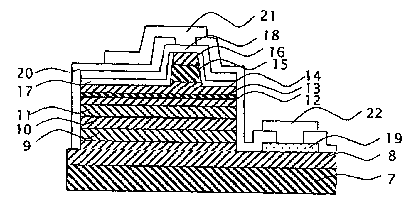
Image

Examples
example 1
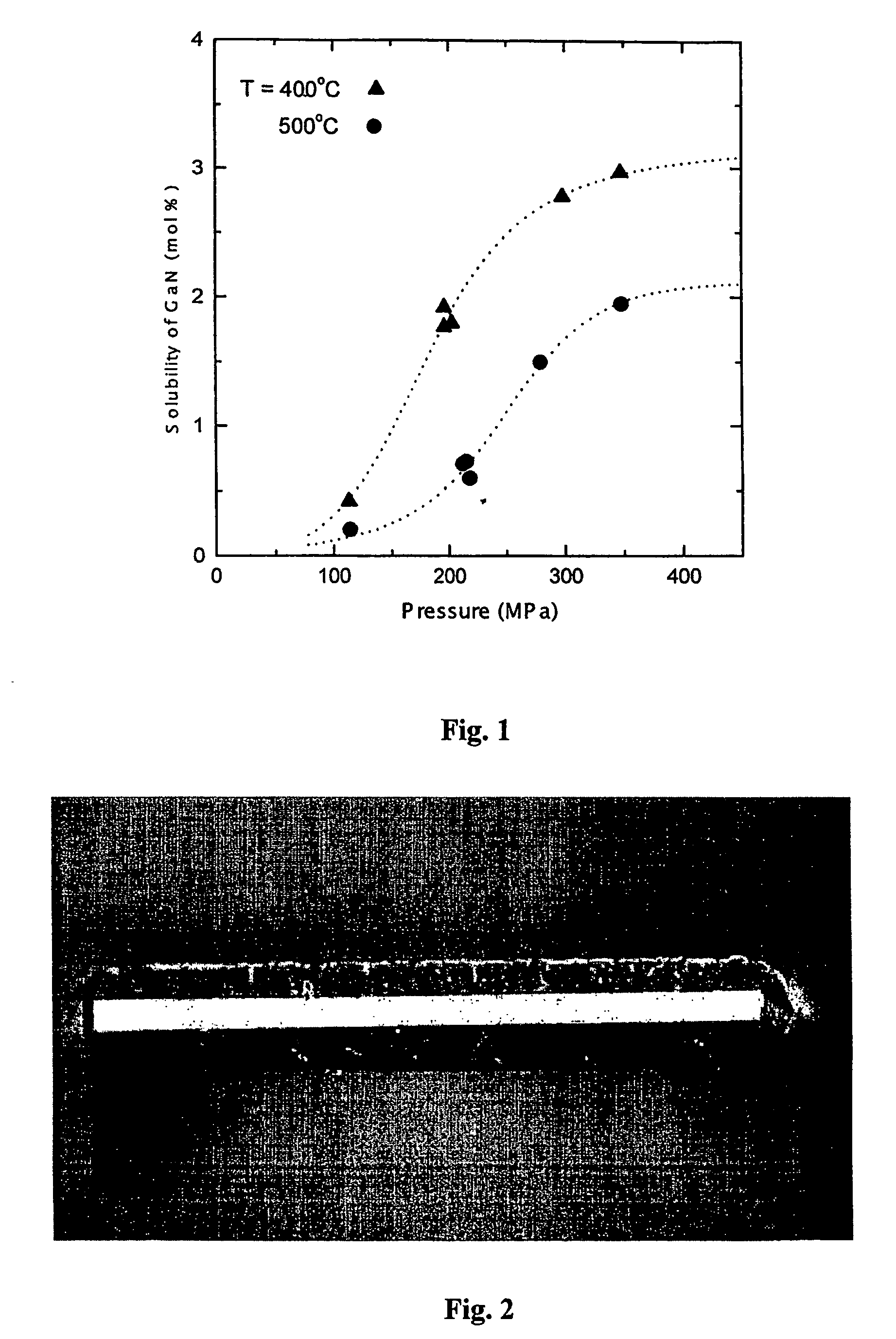
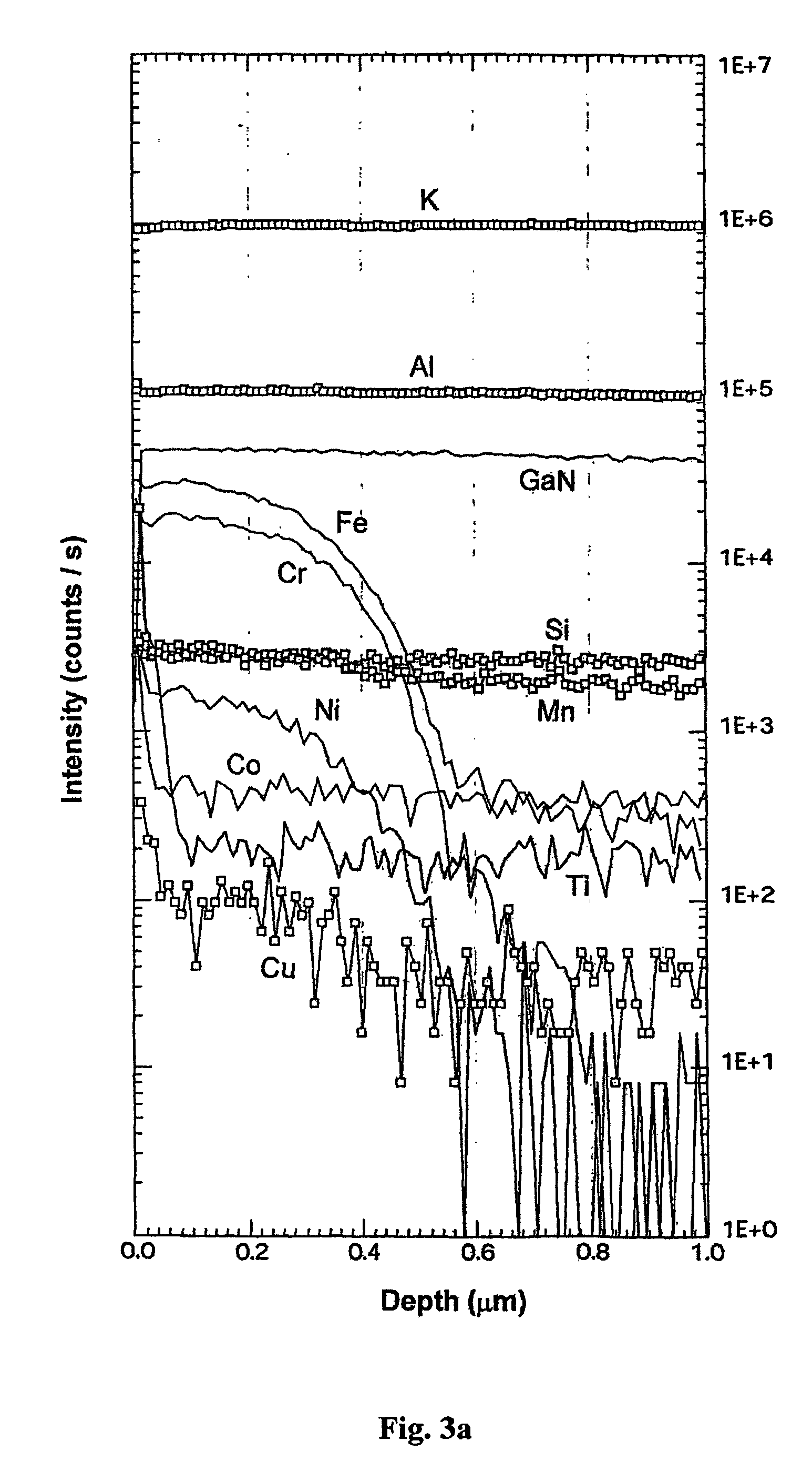
[0095]Two crucibles were introduced into the high pressure 10.9 cm3 autoclave built on the basis of a known design solution [H. Jacobs, D. Schmidt, Current Topics in Materials Science, vol. 8, ed. E. Kaldis (North-Holland, Amsterdam, 1981), 381], one containing 0.4 g feedstock comprising gallium nitride in the form of 0.1 mm thick strips obtained using the HVPE method, second containing a 0.1 g seed crystals with double thickness, also obtained using the HVPE method. 0.72 g 4N purity metallic potassium was introduced into the autoclave. The autoclave was filled with 4.82 g ammonia, and closed. The autoclave was introduced into the oven and heated to 400° C. Pressure inside the autoclave was 200 MPa. The temperature was increased to 500° C. after 8 days, with pressure maintained at 200 MPa. The autoclave was kept under such conditions for another 8 days (graph in FIG. 5). The process led to total dissolution of the feedstock and recrystallization of the gallium nitride layer on the p...
example 2
[0096]Two crucibles were introduced into the 10.9 cm3 high-pressure autoclave, one containing 0.44 g gallium nitride feedstock in the form of 0.1 mm strips obtained using the HVPE method, second containing 0.1 g seed crystals with double thickness, also obtained using the HVPE method. 0.82 g 4N purity metallic potassium was introduced into the autoclave. The autoclave was filled with 5.43 g ammonia, and closed. The autoclave was introduced into the oven and heated to 500° C. Pressure inside the autoclave was 350 MPa. After 2 days, the pressure was decreased to 200 MPa, and temperature was maintained at 500° C. and the autoclave was kept under these conditions for a further period of 4 days (graph in FIG. 6). The process led to total dissolution of the feedstock and recrystallization of the gallium nitride layer on the partly dissolved seed crystals.
example 3
[0097]Two crucibles were introduced into the 10.9 cm3 high-pressure autoclave, one containing 0.3 feedstock in the form of 6N purity metallic gallium, second containing 0.1 g seed crystals obtained using the HVPE method. 0.6 g 4N purity metallic potassium was introduced into the autoclave. The autoclave was filled with 4 g ammonia, and closed. The autoclave was introduced into the oven and heated to 200° C. The temperature was increased after 2 days to 500° C., maintaining pressure at 200 MPa. The autoclave was kept under these conditions for a further period of 4 days (graph in FIG. 7). The process led to total dissolution of the feedstock and recrystallization of the gallium nitride layer on the seed crystals.
PUM
 Abstract
Description
Claims
Application Information