Charge pump phase locked loop
a phase lock and pump technology, applied in the field of electronic circuits, can solve the problems of large area requirements, common mode problems of filters, and not often used filters in integrated applications, and achieve the effects of low spurious emission, high linearity, and fast transmission ga
- Summary
- Abstract
- Description
- Claims
- Application Information
AI Technical Summary
Benefits of technology
Problems solved by technology
Method used
Image
Examples
Embodiment Construction
[0029]The present invention is best understood in relation to FIGS. 3 through 5a–c of the drawings, like numerals being used for like elements of the various drawings.
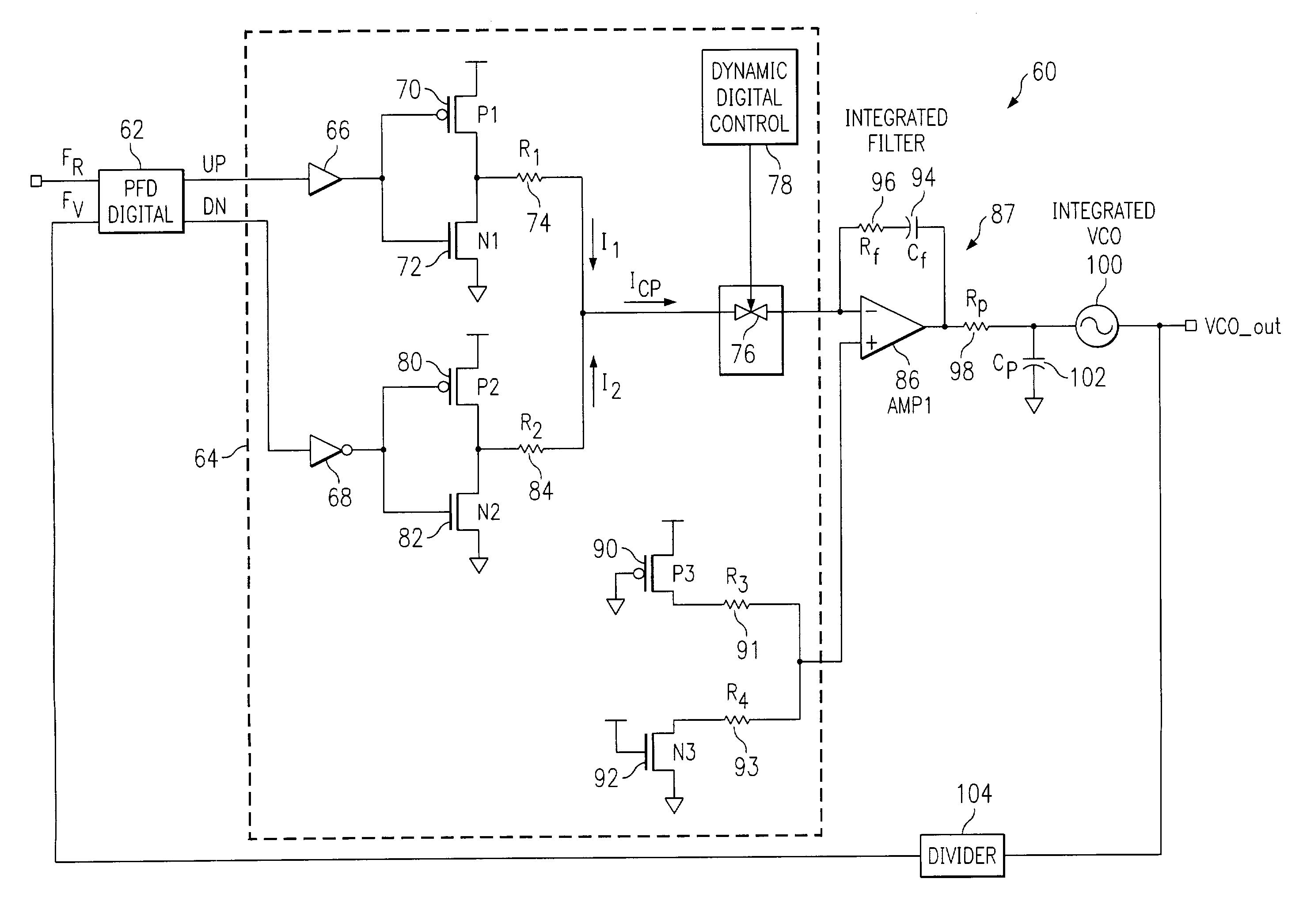
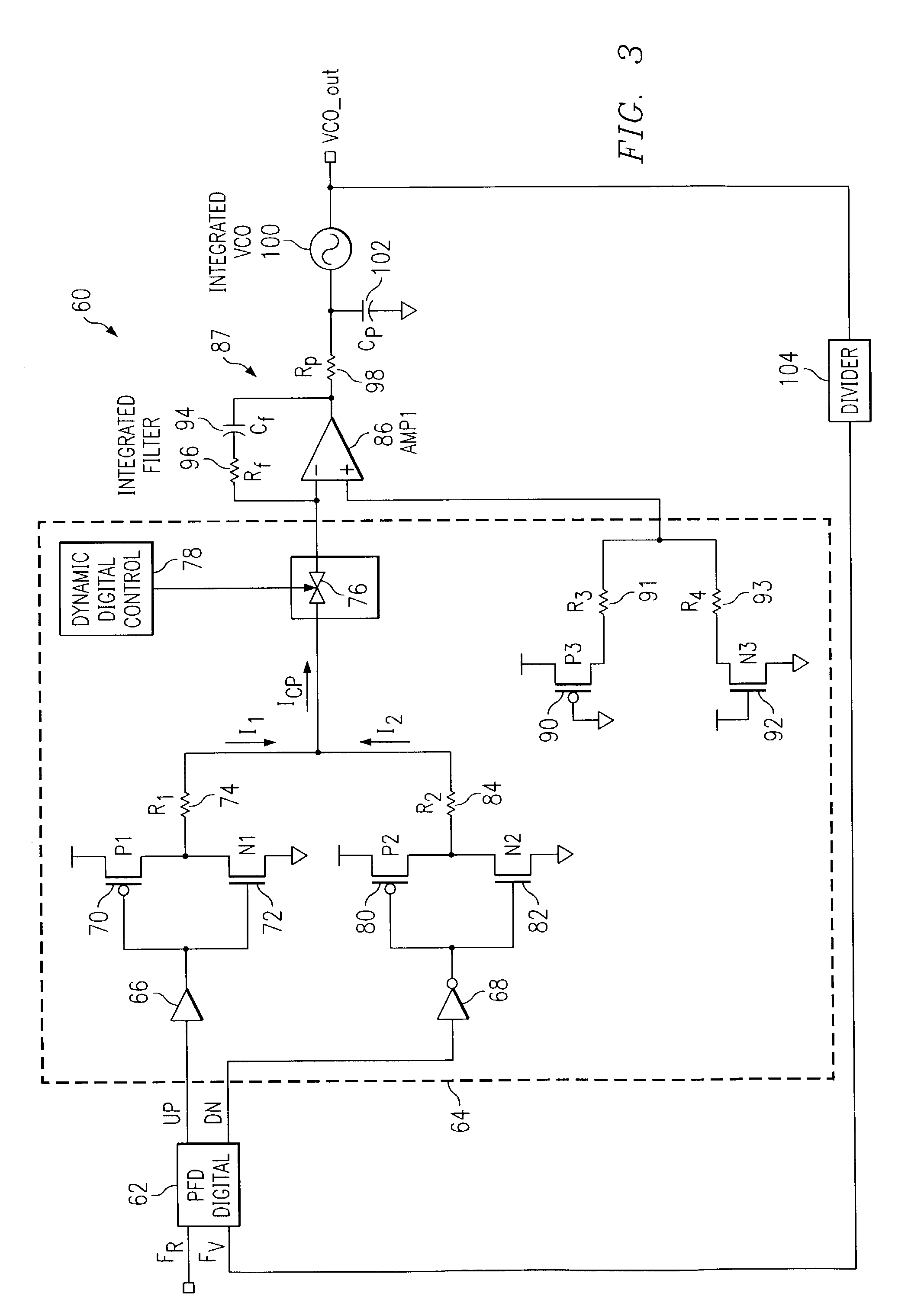
[0030]FIG. 3 illustrates a schematic diagram of a PLL 60 that can be fully integrated on a semiconductor die, with low noise characteristics, low spur levels and high linearity. A reference signal RF is input to PFD 62. PFD 62 outputs UP and DN pulses to a digital charge pump 64. The UP node of PFD 62 is coupled to a non-inverting buffer 66 and the DN node of PFD 62 is coupled to an inverting buffer 68. The output of the non-inverting buffer 66 is coupled to both gates of p-channel transistor 70 and n-channel transistor 72 that produce a logical inversion of the signal at the gates of the transistors. A first source / drain of p-channel transistor 70 is coupled to VDD and a second source / drain of p-channel transistor 70 is coupled to a first source drain of n-channel transistor 72. The second source / drain of n-channel tr...
PUM
 Abstract
Description
Claims
Application Information


