Reference wafer and process for manufacturing same

a technology of reference wafers and manufacturing processes, applied in the field of semiconductor manufacturing, to achieve the effect of very accurate determination

Inactive Publication Date: 2007-01-09
LITEL INSTR
View PDF38 Cites 22 Cited by
  • Summary
  • Abstract
  • Description
  • Claims
  • Application Information

AI Technical Summary

Benefits of technology

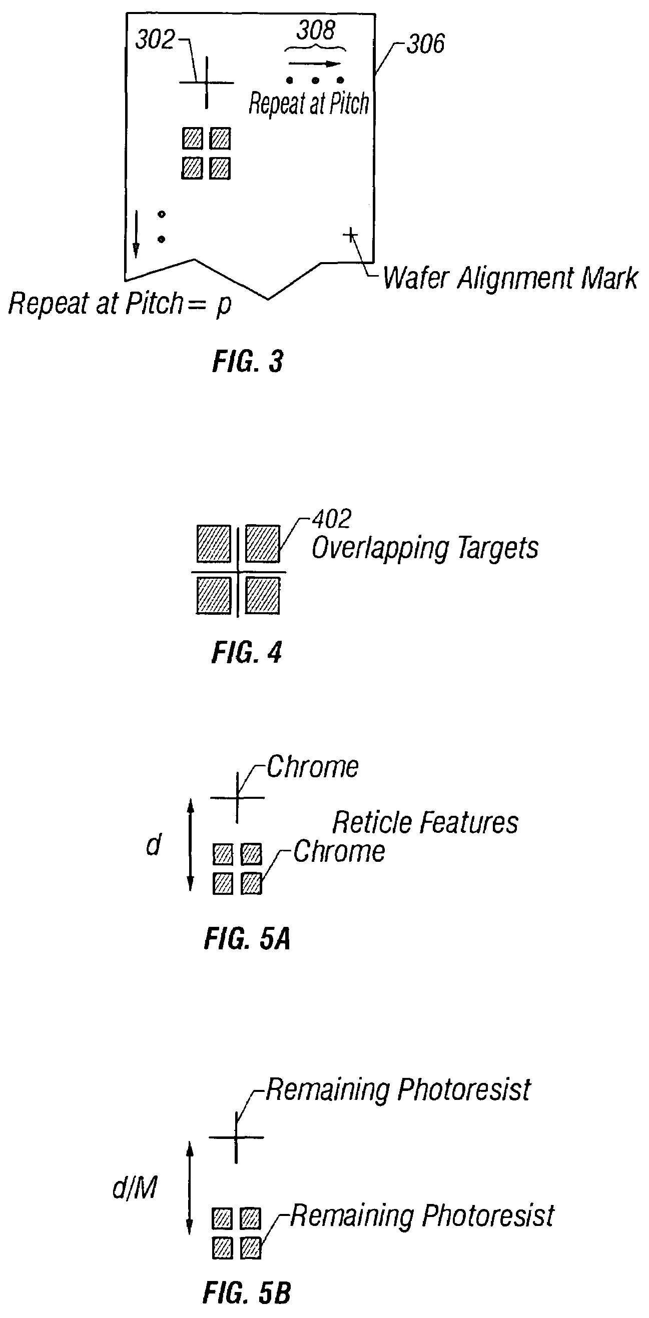
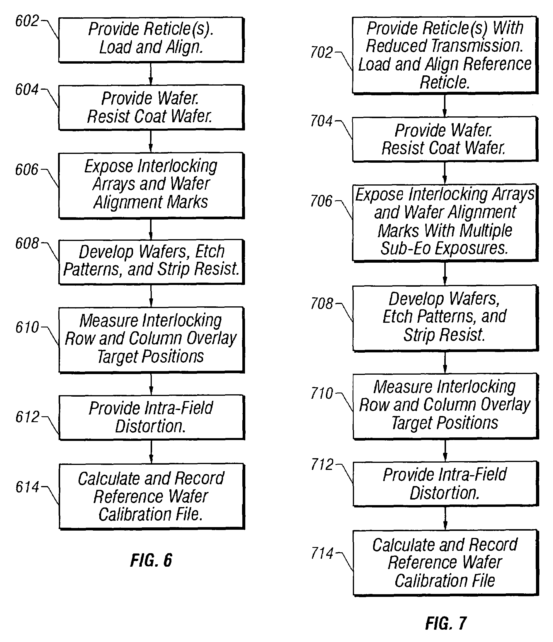
[0013]In accordance with the invention, a process for manufacturing, using, and maintaining a calibrated registration reference wafer for use in semiconductor manufacturing facilities is described. A reference reticle consisting of, for example, a 2-dimensional array of standard alignment attributes is exposed in an interlocking field pattern onto a photoresist coated semiconductor wafer using a photolithographic exposure tool. Following the lithographic development process, the resist patterned wafer is physically etched using standard techniques, thereby creating a permanent record of the alignment attribute exposure pattern. Along the interlocking rows and columns of the resulting wafer, the permanently recorded alignment attributes are measured for placement error using a conventional overlay metrology tool. The resulting overlay error data may be used, for example, in a software program, to generate a unique reference wafer calibration file that contains the positions of all the reference marks (alignment attributes) forming an uninterrupted, regular array across the wafer as well as the wafer alignment marks. The positions of these alignment attributes on the reference wafer can be determined very accurately, except for the possibility of arbitrary translation, rotation, asymmetric scaling and non-orthogonal positional offset errors.

Problems solved by technology

Errors in the overlay measurements due to the exposure of the present machine and not as due to systematic or random errors associated with the machine on which the reference wafer was manufactured.

Method used


Image

  • Reference wafer and process for manufacturing same
  • Reference wafer and process for manufacturing same
  • Reference wafer and process for manufacturing same

Examples


Embodiment Construction

[0066]The effects of overlay error are typically divided into two major categories for the purpose of quantifying overlay error and making precise exposure adjustments to correct the problem. The first category, referred to as grid or rotation 1110 as illustrated in FIG. 11A, or yaw 115 as illustrated in FIG. 11B, of each exposure pattern, exposure field, or simply field, with reference to the nominal center position of the wafer. These global or inter-field positional errors may be caused by the wafer stage subsystem of the photolithographic exposure tool. Overlay modeling algorithms typically divide grid or inter-field error into various sub-categories or components the most common of which are translation, rotation, magnification or scale, non-orthogonality, stage distortion and stage rotation. See Matching Performance for Multiple Wafer Steppers using and Advanced Metrology Procedure, supra.

[0067]The second category, intra-field overlay error is the positional offset of an indiv...


PUM

PropertyMeasurementUnit
stepper projection imagingaaaaaaaaaa
scanning projection imaging systemaaaaaaaaaa
electron beam imagingaaaaaaaaaa

Abstract

An apparatus and method for manufacturing and using a calibrated registration reference wafer in a semiconductor manufacturing facility. A reference reticle consisting of a 2-dimensional array of standard alignment attributes is exposed several times onto a photoresist coated semiconductor wafer using a photolithographic exposure tool. After the final steps of the lithographic development process the resist patterned wafer is physically etched using standard techniques to create a permanent record of the alignment attribute exposure pattern. The permanently recorded alignment attributes are measured for placement error using a conventional overlay metrology tool. The resulting overlay error data is used to generate a calibration file that contains the positions of the alignment attributes on the reference wafer. The reference wafer and calibration file can be used to determine the wafer stage registration performance for any photolithographic exposure tool.

Description

CROSS REFERENCE TO RELATED APPLICATIONS[0001]The present application is a divisional application of U.S. application Ser. No. 10 / 020,569 filed Dec. 7, 2001 now U.S. Pat. No. 6,699,627, entitled “Reference Wafer and Process for Manufacturing Same”. by Adlai Smith, Bruce McArthur, and Robert Hunter, which claims priority to U.S. provisional application Ser. No. 60 / 254,271 filed Dec. 8, 2000, and U.S. patent application Ser. No. 09 / 835,201 filed Apr. 13, 2001, both applications entitled “Method And Apparatus For Self-Referenced Projection Lens Distortion Mapping”, by Adlai Smith, Bruce McArthur, and Robert Hunter, U.S. provisional application Ser. No. 60 / 254,413 filed Dec. 8, 2000 and U.S. patent application Ser. No. 09 / 891,699 filed Jun. 26, 2001, both applications entitled “Method And Apparatus For Self-Referenced Wafer Stage Positional Error”, to Adlal Smith, Bruce McArthur, and Robert Hunter, and U.S. provisional application Ser. No. 60 / 254,315 filed Dec. 8, 2000 entitled “Referenc...

Claims


Application Information

Patent Timeline
Patent Type & Authority Patents(United States)
IPC IPC(8): G03C5/00G03F9/00G03F7/20
CPCG03F7/70558G03F7/70591G03F7/70633G03F7/706Y10S430/168Y10S430/143
Inventor SMITH, ADLAIMCARTHUR, BRUCEHUNTER, JR., ROBERT
Owner LITEL INSTR
Why Eureka
Try Eureka