Tip structures, devices on their basis, and methods for their preparation

Inactive Publication Date: 2007-01-09
CRYSTALS & TECH
View PDF10 Cites 19 Cited by
  • Summary
  • Abstract
  • Description
  • Claims
  • Application Information

AI Technical Summary

Benefits of technology

[0023]Thus, there is a need for a scanning probe device that ensures a stable and fast action in any regimes of its work. In a preferred embodiment, the scanning probe device has a cantilever with a second electrode that applies the resonant modes of oscillations to the lever. This provides an advantageous design of the multi-lever and a non-expensive technology for its production. In a preferred embodiment, components of scanning probe devices (SPD) such as levers, probes on them, can be fractionized and separated from each of other by using a new technology for preparation of tip probes. It is possible to form multifunctional tip structures that allow to combine in a given device, a multilever, several probes with various sensitive components for simultaneous implementation of morphological, electrostatic, magnetic, and chemical investigations.

Problems solved by technology

However, the thermal cathodes consume a lot of energy for their operation.
However, parameters of such emitters are not reproducible because distributions of electric fields between the nanotubes are non-uniform due to their occasional positions.
However, their position at the probe is non-controllable due to their occasional and numerous nucleations.
However, both a shape and a structure of the coatings arc nonoptimal for the high resolution and the high sensitivity of the instruments.
However, both a shape of the tips and a composition of the capacitance material are not optimal for high sensitivity of the instrument.
However, the probes are suitable only for studies of surfaces having rather simple forms such as grooves with vertical walls.
However, there are a lot of cases where surfaces with complicated shapes (such as biological macromolecules) or with a coarse relief must be studied.
There are problems with mapping the spatial arrangement of chemical forces existing on solid surfaces.
Problems with ensuring high scanning rates in SPM devices having a single lever / probe are known.
Due to the small scanning rate, such devices are not broadly used in the industry.
1. In order to realize both feeding / taking-off the levers and tracing their deflections, using only the piezoresistive layers is not sufficient.
2. Creation / production of the multilever devices integrated with multiplexers, operational amplifiers, etc (that is necessary for an effective action of the multi-lever devices) represents a very complicated and expensive technological problem.
This results in the nonresonant damping of the lever oscillations and, finally, in its relaxation.

Method used


Image

  • Tip structures, devices on their basis, and methods for their preparation
  • Tip structures, devices on their basis, and methods for their preparation
  • Tip structures, devices on their basis, and methods for their preparation

Examples


example 1

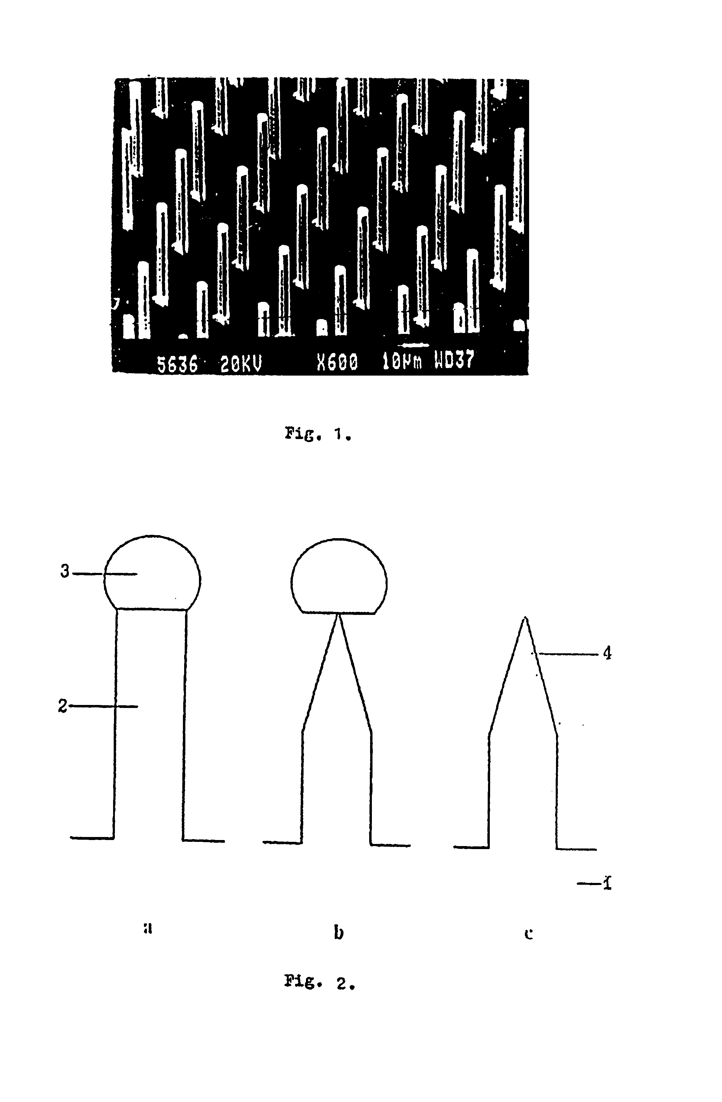
[0106]A beam of argon or nitrogen ions accelerated by electrostatic field 5 kV is directed along the axis of the probe. A conical particle with an angle 40-50° at its apex is formed, as it is shown in FIG. 12. The conical magnetic particle ensures the resolving power of the MFM about 50 nanometers. Calculation has shown that, at such a design of the probe, a contribution of the magnetic film deposited on the basis of the probe into a signal registered by the SPM is at least 100 times less than that of the conical particle deposited onto the tip.

[0107]The magnetic particle prepared by evaporation and, then, treated by the ion beam bombardment has a polycrystalline structure, each magnetic domen formed in a given crystalline grain having its own (arbitrary) direction of magnetization. In order to improve (homogenize) the magnetic properties of the particle, it is subjected to monodomenization by enduring the magnetic probe at a constant magnetic field of a given direction.

[0108]Exampl...

example 2

[0110]A thin film of titanium is deposited onto the silicon tip having the plateau. Then, the film is oxidized by beating to a high temperature in an oxygen-containing atmosphere. A TiO2 coating is formed on the plateau.

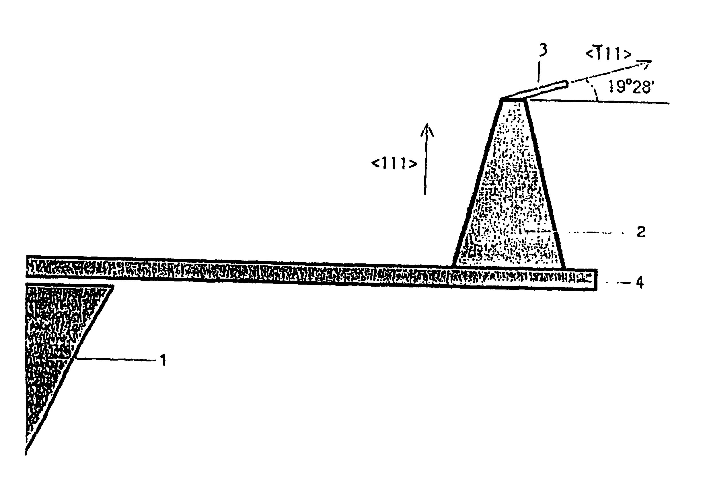
[0111]Other problems that can be solved with the whisker based SPM probes relate to investigations of objects with complicated shapes (such as biological macromolecules, solid surfaces with a course relief, with arbitrary microcavities, etc). For investigations of such objects, a whisker probe having a shape shown in FIG. 15 can be used. The probe consists of at least two parts, a lower one and an upper one. The lower part is formed by a relatively thick silicon whisker perpendicular to a single-crystalline silicon substrate oriented along the most-close-packed crystallographic plane (111) so that it has the orientation . The upper part is formed by another, a more narrow whisker that grows in another, also crystallographic direction that forms the crystallographic a...

example 3

[0116]Silicon whisker is grown by means of a mixture of gold and indium. Accordingly, the solidified globule contains, in addition to silicon, also crystallites of gold and indium. The whisker probe for the chemical force microscopy is coated with an indium film. Owing to the fact that some of indium crystallites of the globule are exposed at its surface, the adhesion of the indium film is enhanced.

[0117]Also, the globule, with the constituent coating or without it, can be coated with various chemical functional groups.


PUM


Abstract

New designs of electron devices such as scanning probes and field emitters based on tip structures are proposed. The tips are prepared from whiskers that are grown from the vapor phase by the vapor-liquid-solid technology. Some new designs for preparation of field-emitters and of probes for magnetic, electrostatic, morphological, etc, investigations based on the specific technology are proposed. New designs for preparation of multilever probes are proposed, too.

Description

FIELD OF THE INVENTION[0001]The invention relates to materials sciences, especially to electronic materials sciences, in particular to microelectronics, especially to mission electronics, to precision instruments for scientific and technological research. More specifically, this invention relates to design and to methods for preparation of electron emissive devices and of scanning probe devices. This invention can also be used in lithographic processes, as well as in basic processes of micro- and nanoelectronics.DESCRIPTION OF THE RELATED ART[0002]Electron emissive devices (EEDs) represent the devices generate flows of electrons in a vacuum for various purposes: for optical imaging, for electron-beam lithography, for lighting, etc. A cathode (an emitter) bearing the flows of electrons represents a principal component of the devices. Thermal cathodes heated to high temperatures serve as a classic example of such devices. However, the thermal cathodes consume a lot of energy for their...

Claims


Application Information

Patent Timeline
IPC IPC(8): C30B25/18B82B1/00C30B29/00G01Q70/12G01Q70/16H01J1/304
CPCB82Y15/00B82Y35/00G01Q70/16H01J1/3042G01Q70/12H01J2201/319
Inventor GIVARGIZOV, EVGENY INVIEVICHGIVARGIZOV, MICHAIL EVGENIEVICH
Owner CRYSTALS & TECH
Why Eureka
Try Eureka