P-type group II-VI semiconductor compounds

a semiconductor compound and iivi technology, applied in the direction of crystal growth process, polycrystalline material growth, chemically reactive gas, etc., can solve the problems and achieve the effect of inhibiting single crystal formation and reducing desired electronic properties

Inactive Publication Date: 2007-01-09
ZENO MATERIALS LLC
View PDF29 Cites 25 Cited by
  • Summary
  • Abstract
  • Description
  • Claims
  • Application Information

AI Technical Summary

Benefits of technology

[0007]The present invention is drawn to a persistent p-type group II-VI semiconductor material. The group II-VI semiconductor is a thin film of a single crystal comprising atoms of group II elements, atoms of group VI elements, and one or more p-type dopants. The p-type dopant concentration is sufficient to provide the desired p-type semiconductor property in a single crystal form. Too much dopant may diminish desired electronic properties and inhibit single crystal formation. The semiconductor resistivity is less than about 0.5 ohm·cm, and preferably much lower. The carrier mobility is greater than about 0.1 cm2 / V·s, and preferably much greater. A persistent p-type group II-VI semiconductor material may be deposited as a thin film on an amorphous, polycrystalline, or crystalline self supporting substrate surface.

Problems solved by technology

Too much dopant may diminish desired electronic properties and inhibit single crystal formation.

Method used


Image

  • P-type group II-VI semiconductor compounds
  • P-type group II-VI semiconductor compounds
  • P-type group II-VI semiconductor compounds

Examples


example 1

Sputtering of ZnO with Arsenic as a Dopant.

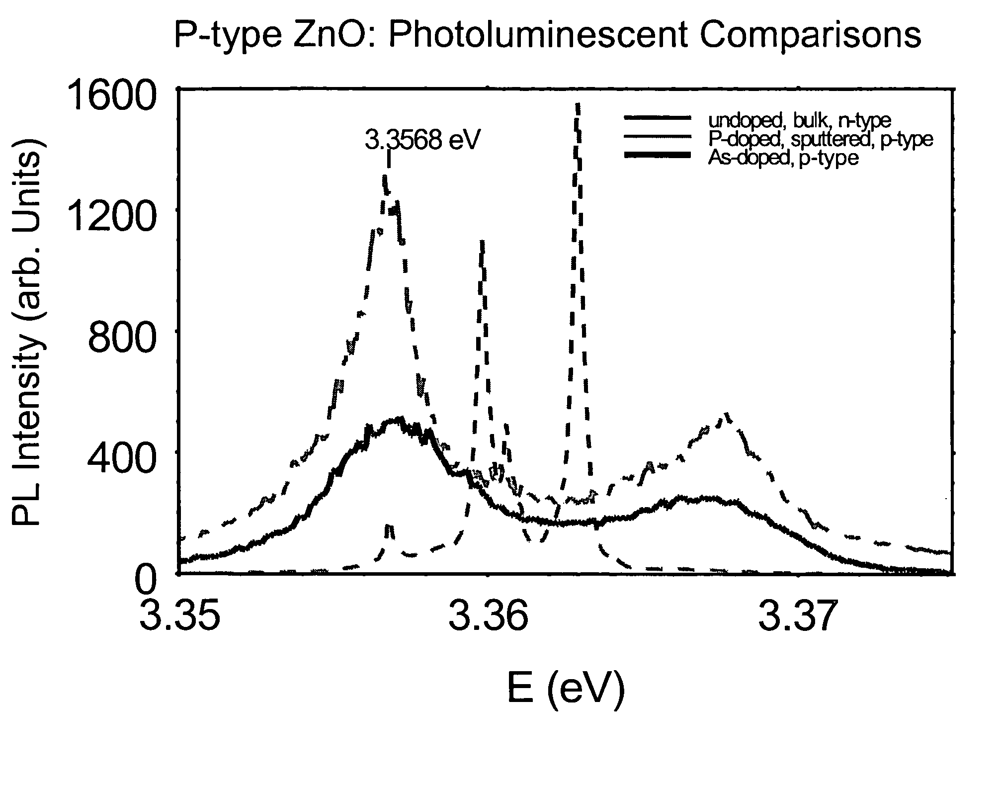
[0063]A thin film of p-type zinc oxide was deposited onto a self supporting substrate by RF sputtering. Both fused silica and silicon wafers were used as the self supporting substrate. The sputtering target composition was ZnO (0.99–0.95 moles)+As (0.01–0.05 moles). The preferred target composition was ZnO (0.98 moles)+As (0.02 moles). The substrate temperature was between 350 and 550° C. The preferred temperature was about 400° C. The RF power was between 20 and 120 watts. The preferred power was about 60 watts. The sputtering atmosphere included argon at a gas pressure of about 4 to 20 mtorr and O2 at a gas pressure of about 1 to 4 mtorr. The preferred sputtering atmosphere pressures were about 9 mtorr argon and about 1 mtorr O2.

[0064]The resulting transparent p-type zinc oxide layer had a resistance of about 10,000 ohms / square. After annealing at 440° C. in air, the resistance dropped to about 1,000 ohms / square. In another composition pr...

example 2

Sputtering of ZnO with Arsenic as a Dopant.

[0065]A thin film of p-type zinc oxide was deposited onto a self supporting substrate by RF sputtering. Both fused silica and silicon wafers were used as the self supporting substrate. The sputtering target composition was ZnO (0.99–0.95 moles)+As (0.01–0.05 moles). The preferred target composition was ZnO (0.98 moles)+As (0.02 moles). The substrate temperature was between 350 and 550° C. The preferred temperature was about 400° C. The RF power was between 20 and 120 watts. The preferred power was about 60 watts. The sputtering atmosphere included argon at a gas pressure of about 4 to 20 mtorr and H2 at a gas pressure of about 1 to 4 mtorr. The preferred sputtering atmosphere pressures were about 9 mtorr argon and about 1 mtorr H2.

[0066]The resulting transparent p-type zinc oxide layer had a resistance of about 500 ohms / square. Without being bound by theory, it is believed that the hydrogen gas may be moderating the concentration of oxygen ...

example 4

Sputtering of ZnO with Arsenic as a Dopant.

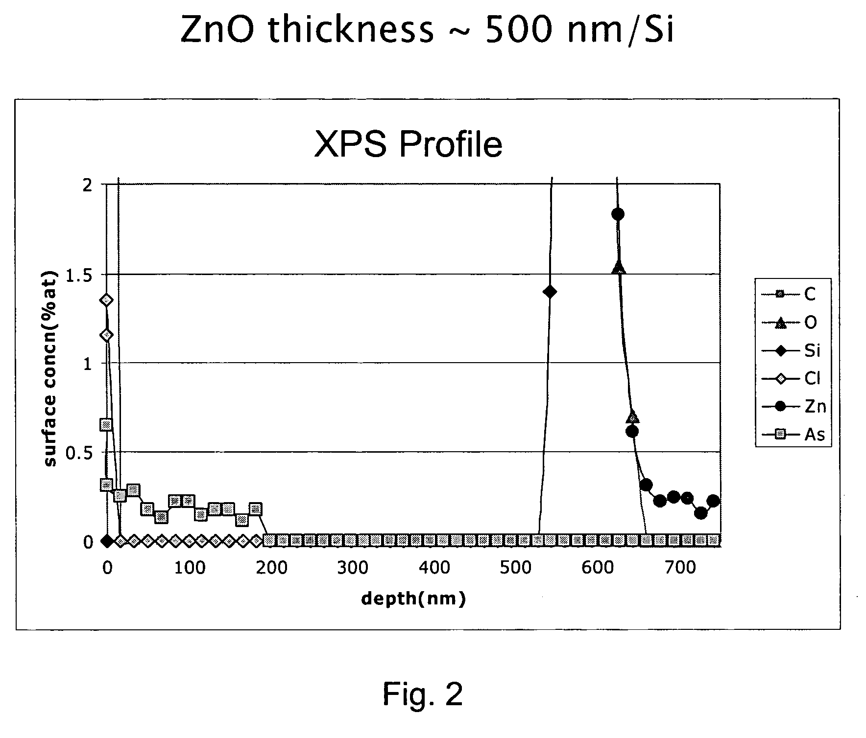
[0069]A thin film of p-type zinc oxide was deposited onto a self supporting substrate by RF sputtering. Both fused silica and silicon wafers were used as the self supporting substrate. A First Composition Layer comprising zinc and arsenic was deposited onto the self supporting substrate.

[0070]In one example, the First Composition Layer was deposited by thermal evaporation of zinc arsenide (Zn3As2 or ZnAs2) for a period of about 2–60 seconds, with a preferred period of about 14 seconds. The substrate temperature was about 360° C. Thermal evaporation is a well known technique for depositing thin films, particularly metal and metal alloys. Subsequent analysis of the First Composition Layer indicated that it contained zinc and arsenic in approximately equal atomic amounts. This suggests that the stoichiometry of the zinc arsenide had changed during thermal evaporation or that it contained a mixture of zinc arsenide molecules.

[0071]The following...


PUM

PropertyMeasurementUnit
carrier mobilityaaaaaaaaaa
semiconductor resistivityaaaaaaaaaa
resistivityaaaaaaaaaa

Abstract

A persistent p-type group II-VI semiconductor material is disclosed. The group II-VI semiconductor includes atoms of group II elements, atoms of group VI elements, and one or more p-type dopants. The p-type dopant concentration is sufficient to render the group II-VI semiconductor material in a single crystal form. The semiconductor resistivity is less than about 0.5 ohm·cm, and the carrier mobility is greater than about 0.1 cm2/V·s. Group II elements include zinc, cadmium, the alkaline earth metals such as beryllium, magnesium calcium, strontium, and barium, and mixtures thereof. Group VI elements include oxygen, sulfur, selenium, tellurium, and mixtures thereof. P-type dopants include, but are not limited to, nitrogen, phosphorus, arsenic, antimony, bismuth, copper, chalcogenides of the foregoing, and mixtures thereof.

Description

CROSS-REFERENCE TO RELATED APPLICATIONS[0001]This application claims the benefit of U.S. Provisional Application No. 60 / 471,916, filed May 20, 2003, U.S. Provisional Application No. 60 / 488,677, filed Jul. 18, 2003, and U.S. Provisional Application No. 60 / 560,428, filed Apr. 8, 2004, which applications are incorporated by reference.BACKGROUND OF THE INVENTION[0002]The present invention provides p-type group II-VI semiconductor compounds.[0003]As used herein, the group II-VI semiconductor compounds include group II elements selected from zinc, cadmium, the alkaline earth metals such as beryllium, magnesium calcium, strontium, and barium, and mixtures thereof, and group VI elements selected from oxygen, sulfur, selenium, tellurium, and mixtures thereof. The group II-VI semiconductor compounds may be doped with one or more p-type dopant. Such p-type dopants include, but are not limited to, nitrogen, phosphorus, arsenic, antimony, bismuth, copper, chalcogenides of the foregoing, and mixt...

Claims


Application Information

Patent Timeline
Patent Type & Authority Patents(United States)
IPC IPC(8): H01L29/12C30B23/02C30B25/02C30B29/48H01L21/363H01L21/365H01L21/368H01L29/22H01L29/225H01L29/227H01L33/28
CPCC30B23/02C30B25/02C30B29/48H01L21/0237H01L21/02554H01L21/02557H01L33/285H01L21/02628H01L21/02631H01L29/22H01L29/225H01L29/227H01L21/02579
Inventor BURGENER, II, ROBERT H.FELIX, ROGER L.RENLUND, GARY M.
Owner ZENO MATERIALS LLC
Why Eureka
Try Eureka