Method for assaying elements in a substrate for optics, electronics, or optoelectronics

a substrate and electronic technology, applied in the field of assaying elements, can solve the problems of dielectric breakdown in future circuits, degrade electrical performance, crystal defect formation, etc., and achieve the effect of improving assaying accuracy and good assaying accuracy

Inactive Publication Date: 2007-01-16
S O I TEC SILICON ON INSULATOR THECHNOLOGIES
View PDF7 Cites 0 Cited by
  • Summary
  • Abstract
  • Description
  • Claims
  • Application Information

AI Technical Summary

Benefits of technology

[0026]The present invention now provides an assaying technique that makes it possible to avoid the drawbacks of the methods described

Problems solved by technology

If a substrate presenting such impurities in the active silicon layer is raised to high temperature, then the impurities can precipitate and thus lead to crystal defects forming.
Such impurities degrade electrical performance, or can lead to dielectric breakdown in future circuits.
In a buried oxide, the presence of contaminants degrades electrical insulation between

Method used


Image

  • Method for assaying elements in a substrate for optics, electronics, or optoelectronics
  • Method for assaying elements in a substrate for optics, electronics, or optoelectronics

Examples


Embodiment Construction

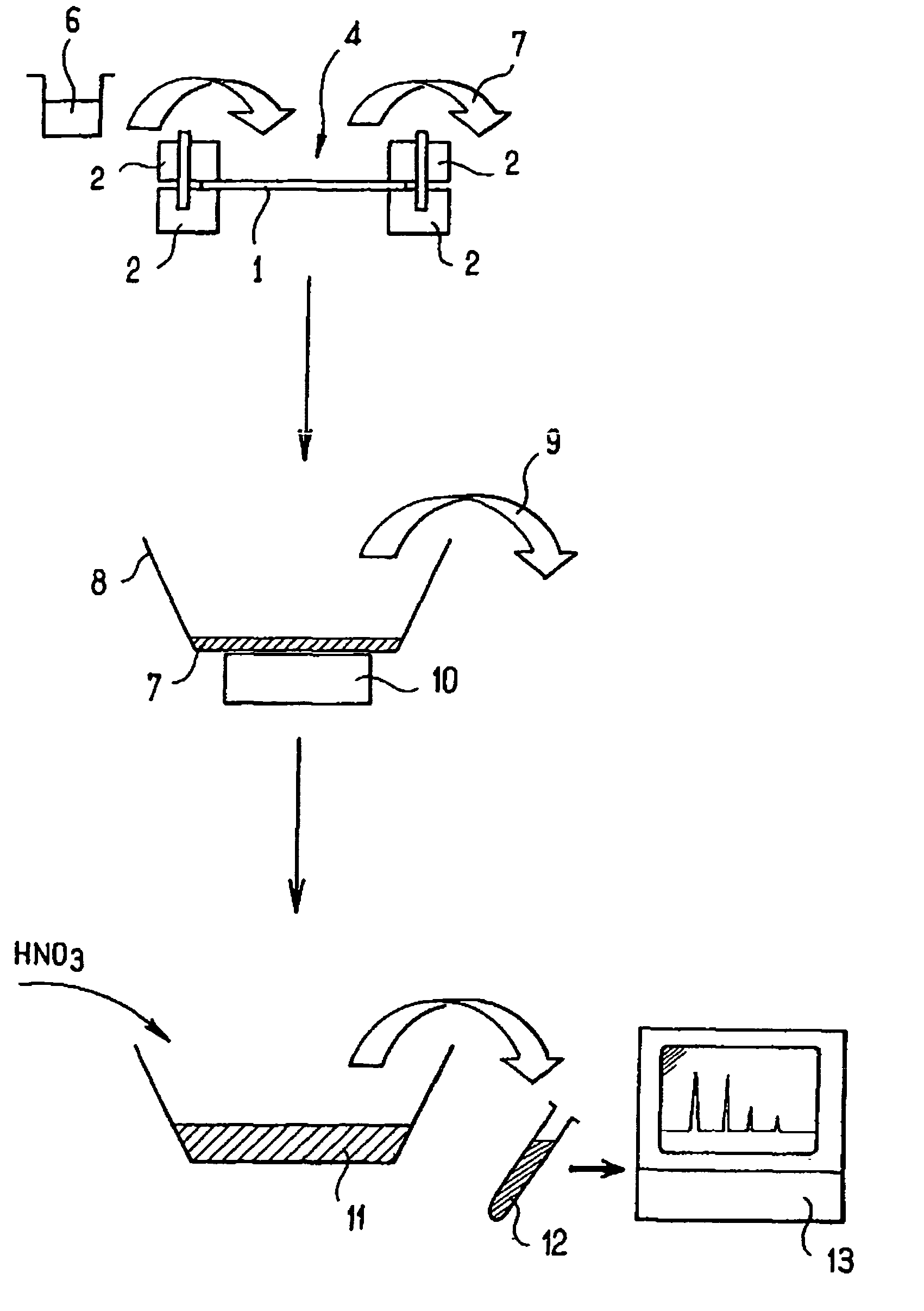
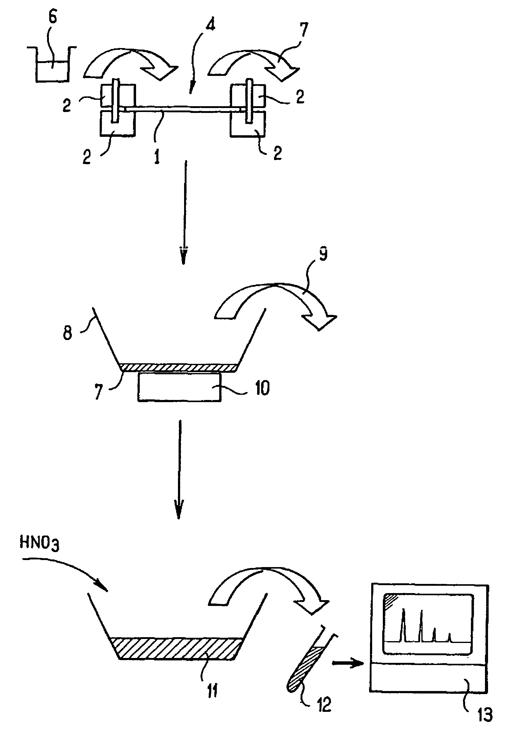
[0040]The invention is based on selective evaporation of the species present in the sample so as to eliminate silicon while retaining the elements that are to be assayed. This enables the concentration of silicon to be reduced to a level compatible with assaying techniques other than AAS. It is thus possible to use faster assaying techniques such as ICPMS. It has also been verified that the silicon depletion obtained by evaporating silicon tetrafluoride using the method of the invention can be performed without losing any significant quantity of the elements that are to be assayed. The assaying method of the invention thus remains very accurate, reliable, and very fast when combined with ICPMS. Furthermore, when combined with an AAS technique, for example, the method has the advantage of improving detection thresholds.

[0041]In further accordance with the invention, the decomposition reaction can be as follows:

Si+HNO3+6HF→H2SiF6+NO2+H2O

[0042]Reference will now be made in detail to th...


PUM

PropertyMeasurementUnit
Temperatureaaaaaaaaaa

Abstract

The invention provides a method of assaying at least one element in a material including silicon. The method includes the steps of decomposing a portion of the material with an etching agent to form a solution containing hexafluorosilicic acid and at least one element to be assayed, heating the solution to a temperature sufficient to transform a substantial portion of the hexafluorosilicic acid into silicon tetrafluoride and to cause at least some of the silicon tetrafluoride to evaporate, such that a solution for assaying is obtained in which the silicon content is reduced while and the elements to be assayed are conserved; and assaying at least one element contained in the solution. The invention is applicable to the field of manufacturing substrates or components for optics, electronics, or optoelectronics, and in particular to the field of quality control.

Description

CROSS-REFERENCE TO RELATED APPLICATION[0001]The application is a continuation of International Application PCT / FR02 / 00521 filed Feb. 12, 2002, the entire content of which is expressly incorporated herein by reference thereto.BACKGROUND[0002]1. Field of the Invention[0003]The invention relates to a method of assaying an element in a material comprising silicon, the material being intended in particular for manufacturing components for optics, electronics, or optoelectronics. For example, the invention can be used for assaying metal elements that might contaminate silicon substrates.[0004]2. Background of the Invention[0005]In silicon technology, the essential component in microelectronics is the metal-oxide-semiconductor (MOS) capacitor. The structure of a MOS capacitor comprises two electrodes (e.g., one made of metal or of polycrystalline silicon, and the other of monocrystalline silicon), separated by a fine insulating layer of silicon oxide (SiO2) referred to as the “dielectric” ...

Claims


Application Information

Patent Timeline
IPC IPC(8): H01L21/461G01N27/62C01B7/19C01B33/107G01N1/40
CPCC01B7/193C01B33/10705G01N1/32G01N1/40G01N2033/0095G01N1/4044G01N2001/4027
Inventor VIRAVAUX, LAURENT
Owner S O I TEC SILICON ON INSULATOR THECHNOLOGIES
Why Eureka
Try Eureka