

Waveguide and microwave ion source equipped with the waveguide
Inactive Publication Date: 2007-01-23
APPLIED MATERIALS INC
View PDF15 Cites 2 Cited by
- Summary
- Abstract
- Description
- Claims
- Application Information
AI Technical Summary
Benefits of technology
[0008]The present invention was made with the foregoing problems of the conventional art in mind, and objects of the present invention are to provide a waveguide which is capable of efficiently guiding an electromagnetic wave such as a microwave and is highly durable physically and chemically, and a microwave ion source which uses the waveguide.
[0010]In the waveguide of the present invention, the waveguide main body is made of a boron nitride or an aluminum oxide, and the outer peripheral surface of the waveguide main body is covered with a thin film made of a titanium nitride, whereby the outer peripheral surface of the waveguide main body and the thin film are sufficiently bonded to each other. Thus, reflection of an electromagnetic wave such as a microwave on the outer peripheral surface of the waveguide main body can be sufficiently suppressed, whereby high-level conductivity can be achieved. Additionally, a combination of the waveguide main body and the thin film makes peeling-off difficult and deterioration thereof caused by a difference in coefficients of thermal expansion between both. Thus, it is possible to maintain the high-level conductivity for a long time.
[0011]In the waveguide of the present invention, there is no particular limitation on a shape of the waveguide main body because the outer peripheral surface of the waveguide main body is covered with the thin film. Thus, flexibility of designing or processing can be improved compared with a waveguide in which the core material is inserted into the metal tube. For example, even in the case of providing a curve of a predetermined angle to the waveguide main body or a special shape such as a wedge shape, it is possible to obtain a highly conductive waveguide.
[0012]In the waveguide of the present invention, preferably, the waveguide main body is made of a boron nitride. By combining the waveguide main body made of a boron nitride with the thin film made of a titanium nitride, it is possible to achieve higher conductivity, better adhesion, improved peeling prevention and longer durability with respect to prior waveguides.
[0014]Thus, by using the waveguide of the present invention as a waveguide of a microwave ion source, it is possible to maintain high conductivity with respect to a microwave for a long time, and to carry out efficient plasma generation by microwave discharging.
Problems solved by technology
Additionally, a combination of the waveguide main body and the thin film makes peeling-off difficult and deterioration thereof caused by a difference in coefficients of thermal expansion between both.
Method used
View moreImage
Smart ImageViewing Examples

Examples
example 1
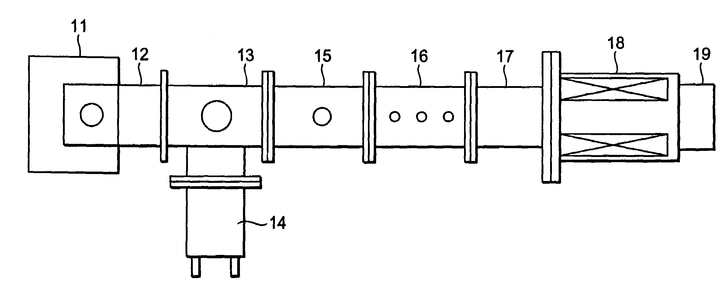
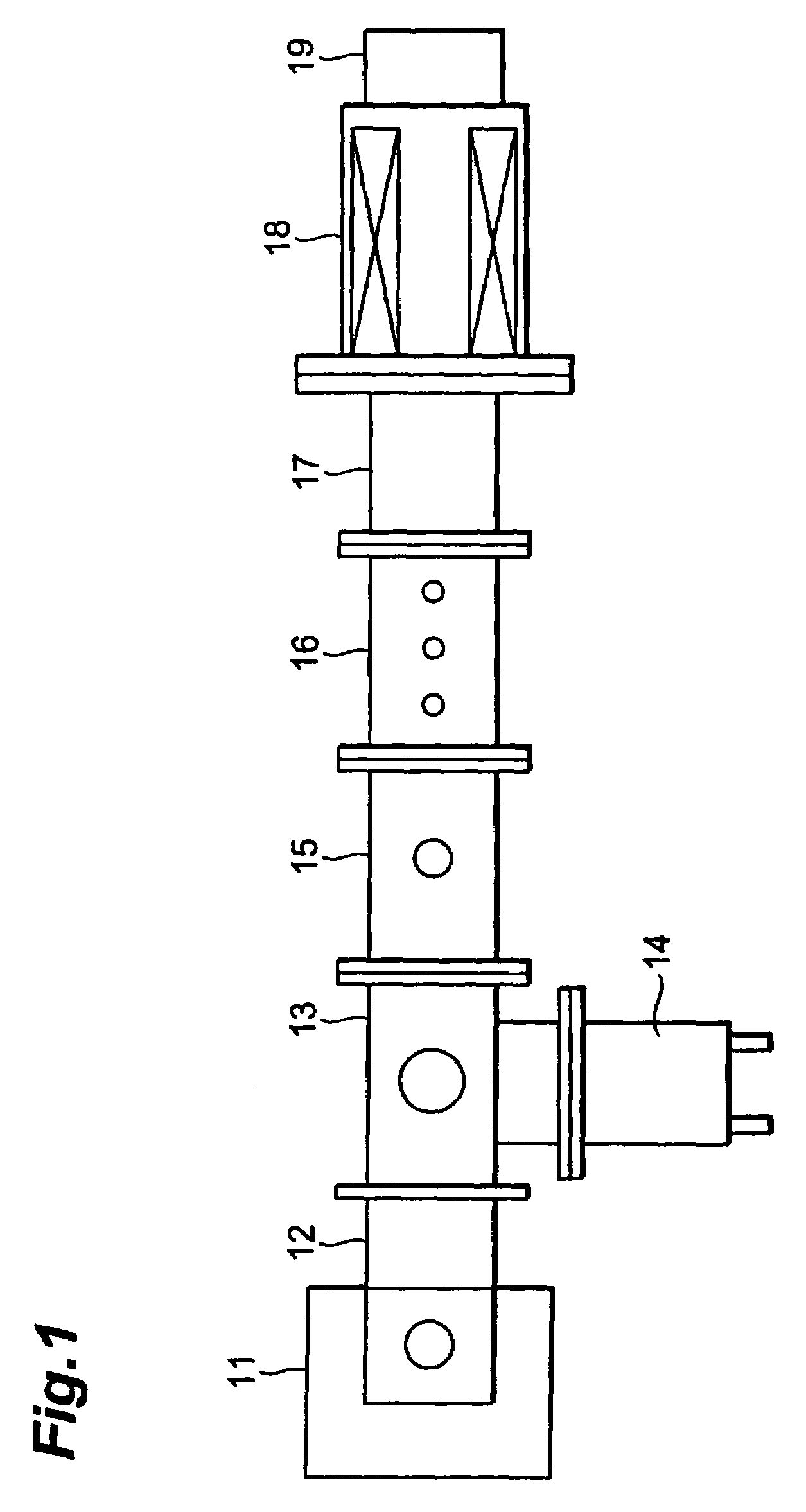
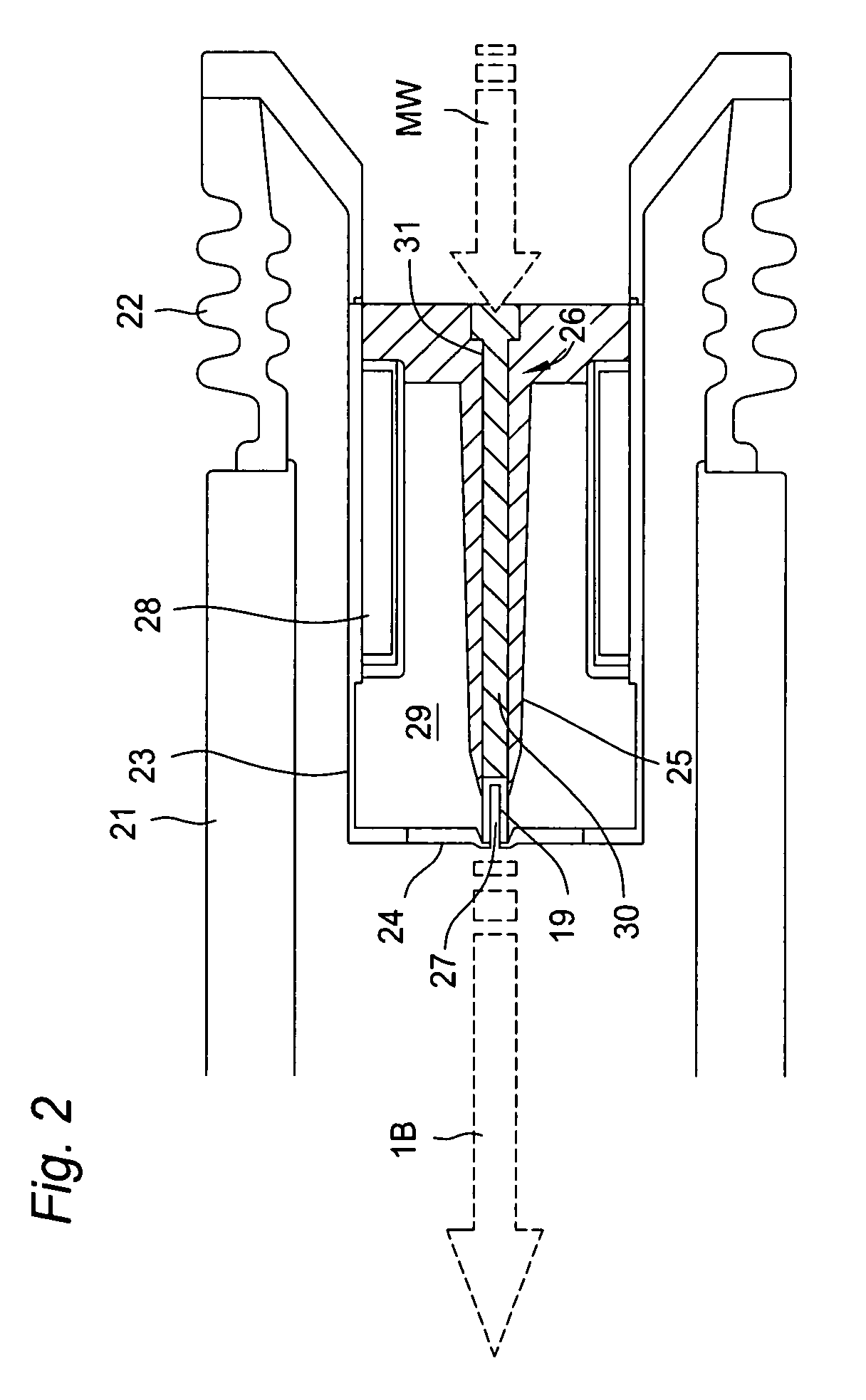
[0029]TiN was deposited on the outer peripheral surface of a waveguide main body made of BN by a CVD method to manufacture a waveguide 26 (thickness of TiN thin film: 200 μm) shown in FIG. 2. Then, the waveguide 26 was used to manufacture a microwave ion source as shown in FIGS. 1 and 2.
Login to View More PUM
| Property | Measurement | Unit |
|---|---|---|
| Thickness | aaaaa | aaaaa |
| Thickness | aaaaa | aaaaa |
| Shape | aaaaa | aaaaa |
Abstract
A waveguide of the present invention comprises a waveguide main body made of a material selected from a boron nitride or an aluminum oxide, and a thin film made of a titanium nitride to cover an outer peripheral surface of the waveguide main body. The waveguide of the present invention can efficiently guide an electromagnetic wave such as a microwave, and has high physical and chemical durability.
Description
BACKGROUND OF THE INVENTION[0001]1. Field of the Invention[0002]The present invention relates to a waveguide and a microwave ion source.[0003]2. Description of the Related Art[0004]Conventionally, a waveguide has widely been used to guide an electromagnetic wave such as a microwave. As such a waveguide, a waveguide has generally been known, in which a core material made of a nonconductor is inserted into a metal tube molded in a cylindrical shape, and an inner peripheral surface of the metal tube and an outer peripheral surface of the core material are bonded to each other. A waveguide has also been known, in which an outer peripheral surface of a nonconductor is covered with a thin film made of a metal such as aluminum or copper (e.g., see Japanese Patent Laid-Open SHO 62 (1987)-278802).[0005]However, there is room for improvement in all the conventional waveguides when they are applied to microwave ion sources or the like.[0006]That is, in the case of the waveguide in which the co...
Claims
Login to View More Application Information
Patent Timeline
 IPC IPC(8): H01J7/24C23C16/00G21K1/08H01J3/14H01J3/26H05B31/26G21K1/00H01J27/16H01J37/08H01P3/12H05H1/46H05H7/08
CPCH01J37/08H01P3/12H01J2237/0817
InventorITO, HIROYUKISAKUDO, NORIYUKI
OwnerAPPLIED MATERIALS INC