Method of treatment of porous dielectric films to reduce damage during cleaning

a dielectric film and porous technology, applied in the direction of cleaning using liquids, instruments, semiconductor/solid-state device details, etc., can solve the problems of difficult to clean resist or residues from low-k dielectric materials without affecting the low-k dielectric material, and large residues and polymers are typically left on the sidewalls. , to achieve the effect of reducing the loss of thickness or widening of openings, reducing the loss o

Inactive Publication Date: 2007-01-30
TOKYO ELECTRON LTD
View PDF256 Cites 3 Cited by
  • Summary
  • Abstract
  • Description
  • Claims
  • Application Information

AI Technical Summary

Benefits of technology

[0015]The preferred embodiment of the current invention is for use in conjunction with supercritical carbon dioxide (SCCO2). In alternate embodiments of the current invention, a dry chemical ion-depleted downstream microwave plasma approach is utilized. In yet another embodiment of the current invention, a wet chemical process is utilized in conjunction with the current invention to achieve high...

Problems solved by technology

Stripping is a limitation due to the fact that a polymer is utilized for the low-k and an organic resist.
Cleaning the resist or residues from low-k dielectric materials without affecting the low-k dielectric material is complicated.
However, considerable resid...

Method used


Image

  • Method of treatment of porous dielectric films to reduce damage during cleaning
  • Method of treatment of porous dielectric films to reduce damage during cleaning
  • Method of treatment of porous dielectric films to reduce damage during cleaning

Examples


Embodiment Construction

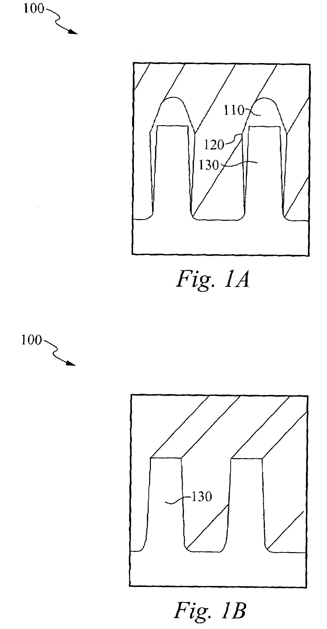
[0021]Materials exhibiting low dielectric constants of between 3.5–2.5 are generally referred to as low-k dielectric materials. Porous materials with dielectric constant of 2.5 and below are generally referred to as ultra low-k (ULK) dielectric materials. For the purpose of this application low-k dielectric materials refer to both low-k dielectric and ultra low-k dielectric materials. Low-k dielectric materials are usually porous oxide-based materials and can include an organic or hydrocarbon component. Examples of low-k dielectric materials include, but are not limited to, carbon-doped oxide (COD), spin-on-glass (SOG) and fluorinated silicon glass (FSG) materials. These porous low-k dielectric material films typically contain carbon and hydrogen and are deposited by methods such as spin-on or CVD. These films are processed in such a way as to produce a film resistant to damage from cleaning formulations and typically have an inorganic matrix of either a SiOx base or a SiOx-CxHy bas...


PUM

PropertyMeasurementUnit
Temperatureaaaaaaaaaa
Pressureaaaaaaaaaa
Dielectric polarization enthalpyaaaaaaaaaa

Abstract

A device, method, and system for treating low-k dielectric material films to reduce damage during microelectronic component cleaning processes is disclosed. The current invention cleans porous low-k dielectric material films in a highly selectivity with minimal dielectric material damage by first treating microelectronic components to a passivating process followed by a cleaning solution process.

Description

RELATED APPLICATION(S)[0001]This Patent Application is a continuation in part of U.S. patent application, Ser. No. 10 / 379,984, filed on Mar. 4, 2003, and entitled “METHOD OF PASSIVATING OF LOW DIELECTRIC MATERIALS IN WAFER PROCESSING”. This Patent Application claims priority under 35 U.S.C. 119(e) of the U.S. Provisional Patent Application, Ser. No. 60 / 372,822 filed Apr. 12, 2002, and entitled “METHOD OF TREATMENT OF POROUS DIELECTRIC FILMS TO REDUCE DAMAGE DURING CLEANING”. The Provisional Patent Application, Ser. No. 60 / 372,822 filed Apr. 12, 2002, and entitled “METHOD OF TREATMENT OF POROUS DIELECTRIC FILMS TO REDUCE DAMAGE DURING CLEANING”, and the U.S. patent application Ser. No. 10 / 379,984, filed Mar. 4, 2003, and entitled “METHOD OF PASSIVATING OF LOW DIELECTRIC MATERIALS IN WAFER PROCESSING” are also hereby incorporated by reference.FIELD OF THE INVENTION[0002]This invention relates to the field of cleaning of dielectric films. More particularly, this invention relates to sy...

Claims


Application Information

Patent Timeline
IPC IPC(8): G03F7/00B08B7/00C03C15/00C03C17/30C03C23/00C23C8/10C23C26/00C23C30/00G03F7/42H01L21/3105H01L21/311H01L21/312H01L21/316H01L23/532
CPCB08B7/0021C03C17/30C03C23/0075C23C8/10C23C26/00C23C30/00G03F7/422G03F7/423H01L21/02126H01L21/02343H01L21/3105H01L21/31058H01L21/31116H01L21/3121H01L21/3125H01L21/316H01L21/31629H01L21/31633C03C15/00H01L23/5329H01L21/31695H01L2924/0002H01L2924/00
Inventor SCHILLING, PAUL
Owner TOKYO ELECTRON LTD
Why Eureka
Try Eureka