Forming method of silicide film

Inactive Publication Date: 2007-02-13
LAPIS SEMICON CO LTD
View PDF13 Cites 0 Cited by
  • Summary
  • Abstract
  • Description
  • Claims
  • Application Information

AI Technical Summary

Benefits of technology

[0016]In this way, by forming the titanium nitride film using the titanium target from which the nitride film on it surface has been previously removed, titanium effectively reduces the natural oxide film on the active layer during the heat treatment and the excellent silicification can be occurred.
[0018]The target-cleaning method is a process that gas is evacuated from a processing chamber, then the sputter treatment is performed on the titanium target, and thus titanium nitride on the titanium target is removed. In this manner, the nitride film on the titanium target can be removed easily.
[0024]The unreacted titanium contained in the titanium nitride film can be ensured sufficiently by performing the sputter treatment under such low temperature conditions.
[0028]Thus, in the steps from the formation of the cobalt film to the first annealing treatment, since the substrate is not required to be carried out in the atmosphere, the oxidation of the titanium nitride film containing titanium as the cap film can be prevented and the excellent silicide film can be formed.

Problems solved by technology

However, a single titanium film is not preferable for the cap film.
It is because the single titanium also forms an alloy of cobalt and titanium, leading to difficulty for control of a thickness of cobalt silicide.

Method used


Image

  • Forming method of silicide film
  • Forming method of silicide film
  • Forming method of silicide film

Examples


first embodiment

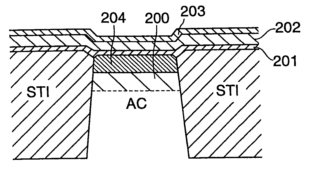
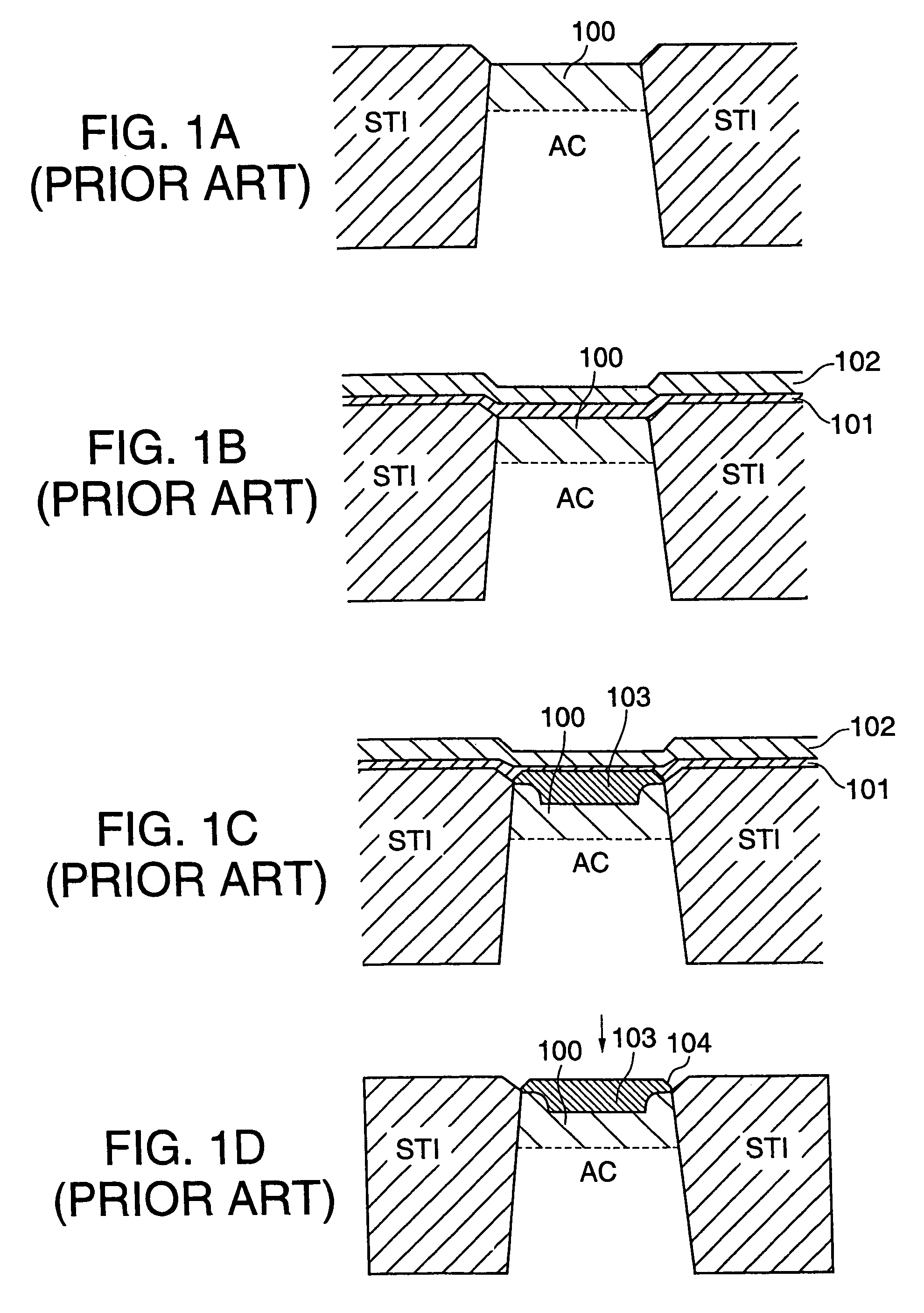
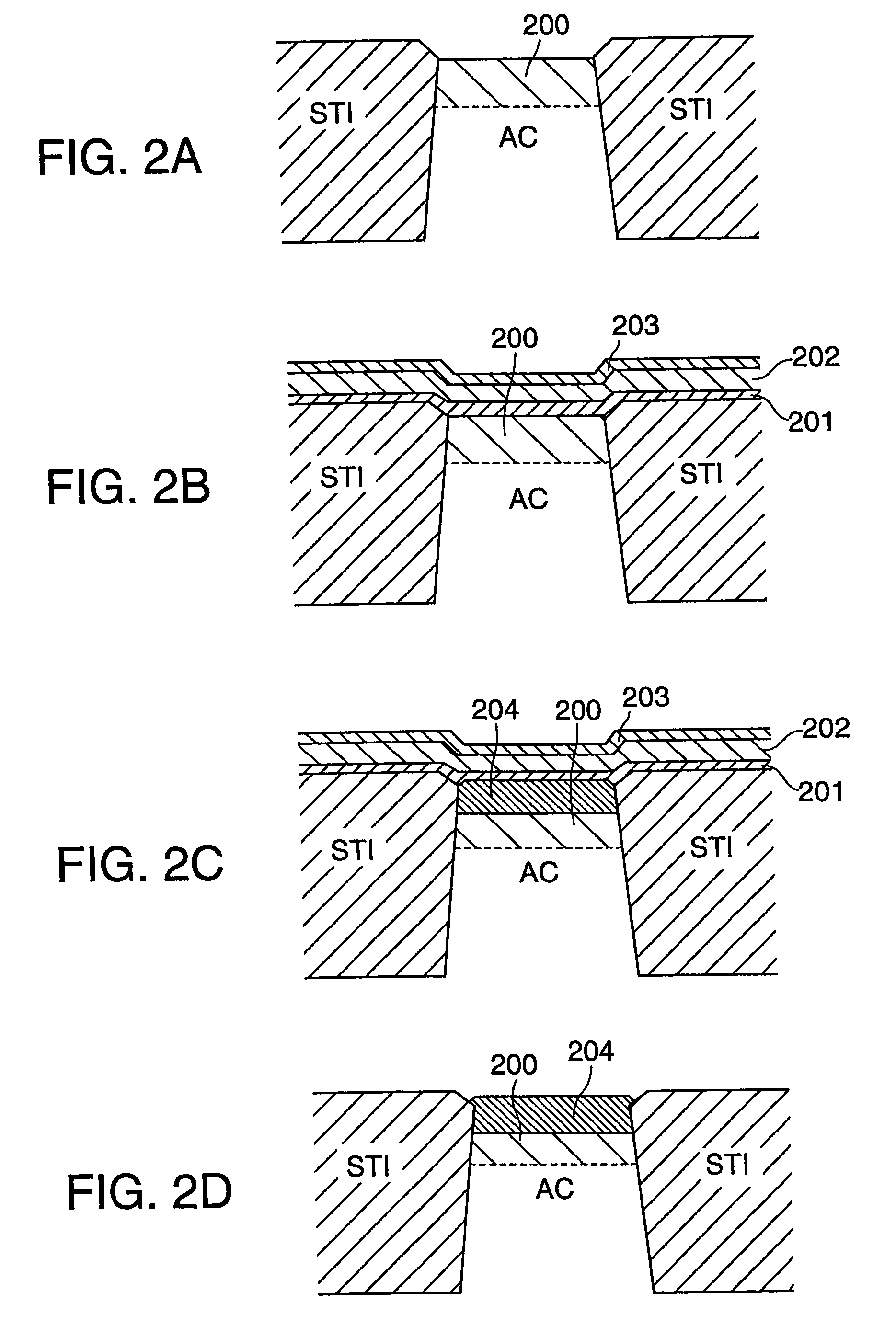
[0034]The first embodiment of the invention is shown in FIG. 2. First, the silicon substrate is isolated using the conventional technique, the STI area and active area are formed, and the diffusion layer 200 is formed in the active area (FIG. 2A). Subsequently, the treatment of the ammonia peroxide mixture and buffered fluorinate acid is done for 60 seconds (this is corresponding to the etching conditions of the thermal oxidation film of 20 Å), in addition, isopropylalcohol-drying is performed.

[0035]Next, following steps are performed successively by the multi-chamber sputter equipment. First, the degassing is done, next the sputter-cleaning is done, then the cobalt film 201 is deposited in 60 Å, and the titanium nitride film is deposited in 200 Å. Herein, conditions of the processes except for the sputter step of titanium nitride are the same as that of the prior art: the degassing is done at 300° C. for 60 seconds, and the sputter-cleaning is done under the conditions that RF (60 ...

second embodiment

[0040]The second embodiment of the invention is shown in FIG. 3. The silicon substrate is isolated using the conventional technique, the STI area and the active area are formed, and the diffusion layer 300 is formed in the active area (FIG. 3A). Subsequently, in order to remove the natural oxidation film on the diffusion layer 300, the treatment of the ammonia peroxide mixture and buffered hydrofluoric acid is performed for 60 seconds (this is corresponding to the etching conditions of the thermal oxidation film of 20 Å), in addition, the isopropylalcohol-drying is performed.

[0041]Next, the following steps are performed successively by the multi-chamber sputter equipment. First the degassing is done, next the sputter-cleaning is done, then the cobalt film 301 is deposited in 60 Å, the titanium film 302 is deposited in 50 Å, the titanium nitride film 303 is deposited in 300 Å, and the titanium film 304 is deposited in 50 Å (FIG. 3B). Herein, for the respective treatment conditions, t...

third embodiment

[0046]The construction of the equipment for use in the third embodiment of the invention is shown in FIG. 4. Each of chambers has been evacuated. Herein, the method for achieving the first embodiment is described using the equipment shown in FIG. 4. The silicon substrate is isolated using the conventional technique and the STI area and the active area are formed, as shown in FIG. 2A. Herein, in order to remove the natural oxide film on the diffusion layer 200 formed in the active area, the treatment of the ammonia peroxide mixture and buffured hydrofluoric acid is done for 60 seconds (this is corresponding to the etching conditions of the thermal oxidation film of 20 Å), in addition, the isopropylalcohol-drying is performed.

[0047]Next, the substrate is introduced into a load lock chamber 401 (or the load lock chamber 402), and introduced into a preheat chamber 404 via a separation chamber 403, and then the degassing is done, for example, at 300° C. for 60 seconds. Then, it is transf...


PUM


Abstract

A manufacturing method of a semiconductor device includes forming a cobalt film on a silicon substrate on which a diffusion layer is formed, forming a titanium film on the cobalt film using a titanium target having a surface from which a nitride film has previously been removed, forming a titanium nitride film containing titanium on the cobalt film by a reactive sputtering process using a nitrogen gas and the titanium target, and performing an annealing to react the cobalt film with the silicon substrate, thereby accomplishing silicification.

Description

CROSS REFERENCE TO RELATED APPLICATIONS[0001]This is a divisional application of application Ser. No. 10 / 233,435, filed Sep. 4, 2002 now abandonded, which is hereby incorporated by reference in its entirety for all purposes.BACKGROUND OF THE INVENTION[0002]1. Field of the Invention[0003]The present invention relates to a forming method of a silicide film, i.e., a method for forming an excellent cobalt silicide film, and particularly, it relates to a formation of titanium nitride on a cobalt film.[0004]2. Description of Related Art[0005]A typical method for forming cobalt silicide will be described with reference to FIG. 1. First, a silicone substrate is subjected to element separation by the use of a conventional technique to form a shallow trench isolation (STI) area and an active area in which a diffusion layer 100 is formed (FIG. 1A).[0006]Subsequently, a natural oxide film on the diffusion layer 100 is removed as a pretreatment for depositing a cobalt (Co) film 101. The oxide fi...

Claims


Application Information

Patent Timeline
IPC IPC(8): H01L21/44H01L21/28H01L21/285
CPCH01L21/02057H01L21/2855H01L21/28518
Inventor HASHIMOTO, KEIICHI
Owner LAPIS SEMICON CO LTD
Why Eureka
Try Eureka