Method of fabricating trench junction barrier rectifier

a technology of trench junction and barrier rectifier, which is applied in the field of metal-emiconductor rectifying devices, can solve the problems of reducing circuit efficiencies, increasing power loss, and reducing the turn off time of the diode, so as to reduce the area consumed by the trenches and by the lateral diffusion of the pn junction, and reduce the lateral diffusion of boron along the semiconductor surfa

Inactive Publication Date: 2007-03-06
SILICONIX
View PDF17 Cites 63 Cited by
  • Summary
  • Abstract
  • Description
  • Claims
  • Application Information

AI Technical Summary

Benefits of technology

[0018]To ensure good electrical performance of the diode, the area consumed by the trenches and by the lateral diffusion of the PN junction should be minimized. In a preferred fabrication method, the region of second conductivity type adjoining the trenches is formed by a diffusion of boron atoms from boron doped polysilicon into the side walls and into the bottom of the trench. The polysilicon itself can be doped in-situ during the deposition in a chemical vapor deposition (CVD) process, or the polysilicon can be doped by implantation. In the case of the implanted polysilicon, the choice of the fabrication method plays an important role.
[0019]In a preferred fabrication method, the trench is filled with polysilicon and the polysilicon is etched back. After etch-b...

Problems solved by technology

Conventional silicon PN-junction diodes have a number of disadvantages, including: (i) a large voltage drop of approximately 700 mV or more, depending on the operating current density when the diode is in its forward conducting state, and (ii) the diode's characteristic of storing a large number of minority carriers when it is in the forward-conducting condition, which slows the diode's turn off time and leads to numerous problems relating to diode reverse recovery such as increased power loss, heating, noise and reduced circuit efficiencies.
A major disadvantage of the Schottky diode is its relatively high offstate leakage current, which is typically orders of magnitude higher than the leakage current of a PN junction diode.
However, a higher Schottky barrier leads to a larger forward-voltage drop, which varies linearly with the barrier height.
As a result, conventional planar Schottky diodes are over-designed in the sense of using a doping concentration in the semiconductor that is too low for the requested blocking voltage.
Thus an important issue in the design of a Schottky diode is the optimization of the trade-off between the v...

Method used


Image

  • Method of fabricating trench junction barrier rectifier
  • Method of fabricating trench junction barrier rectifier
  • Method of fabricating trench junction barrier rectifier

Examples


Embodiment Construction

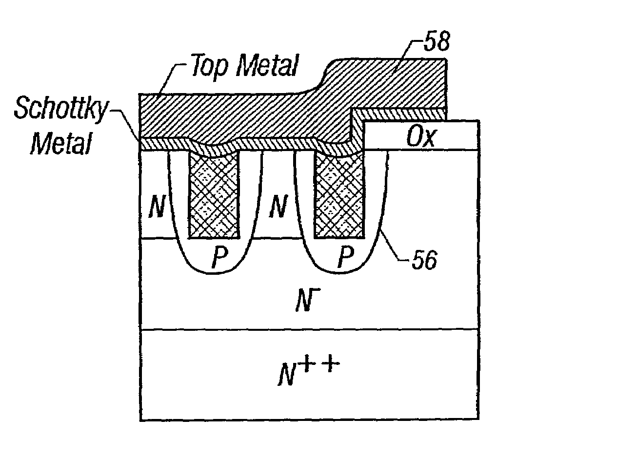
[0042]As described above, an object of this invention is to provide a Schottky diode structure minimizing the barrier lowering effect, integrating an avalanche-rugged PN clamping diode, and allowing easy fabrication.

[0043]An embodiment according to this invention is shown in FIG. 6, which shows a trench junction barrier Schottky diode 10. Schottky diode 10 is formed in an N+ silicon substrate 12, on which an N-epitaxial (epi) layer 14 is grown. Epi layer 14 is subdivided into two layer, designated Nepi1 and Nepi2, each of which has a different doping concentration of N-type atoms. Trenches 16 are formed in the top surface of epi layer 14. A P-type region 18 is formed adjacent each of trenches 16, and region 18 forms a PN junction 20 with the N-type portions of epi layer 14. Trenches 16 are separated by mesas 22 and are filled with polysilicon 24. The top surface of polysilicon 24 is approximately coplanar with the top surfaces of the mesas 22. A metal layer 26, formed of a Schottky ...


PUM


Abstract

A Schottky rectifier includes a rectifying interface between a semiconductor body and a metal layer. Trenches are formed in the surface of the semiconductor body and regions of a conductivity type opposite to the conductivity type of the body are formed along the sidewalls and bottoms of the trenches, the regions forming PN junctions with the rest of the body. When the rectifier is reverse-biased, the depletion regions along the PN junctions merge to occupy the entire width of the mesas. The device is fabricated by implanting dopant directly through the sidewalls and bottoms of the trenches, by filling the trenches with a material containing dopant and causing the dopant to diffuse through the sidewalls and bottoms of the trenches, or by implanting and diffusing the dopant into a gate filling material.

Description

REFERENCE TO RELATED APPLICATION[0001]This application is a divisional of application Ser. No. 09 / 476,389, filed Dec. 30, 1999, abandoned.[0002]This application is related to application Ser. No. 08 / 832,012 filed Apr. 2, 1997, which is incorporated herein by reference in its entirety.FIELD OF THE INVENTION[0003]This invention relates to rectifiers and more specifically to metal-semiconductor rectifying devices, and to methods of fabricating these devices.BACKGROUND OF THE INVENTION[0004]Schottky diodes are employed as rectifiers in numerous power and small signal applications where the forward conduction or switching characteristics of the diode are important. Conventional silicon PN-junction diodes have a number of disadvantages, including: (i) a large voltage drop of approximately 700 mV or more, depending on the operating current density when the diode is in its forward conducting state, and (ii) the diode's characteristic of storing a large number of minority carriers when it is...

Claims


Application Information

Patent Timeline
IPC IPC(8): H01L21/8238H01L21/329H01L27/08H01L29/861H01L29/872
CPCH01L27/0817H01L29/66136H01L29/8725H01L29/861H01L29/872H01L29/66143H01L29/0619
Inventor KOREC, JACEKWILLIAMS, RICHARD K.
Owner SILICONIX
Why Eureka
Try Eureka