Planar extraordinary magnetoresistance sensor

a magnetoresistance sensor, a plane technology, applied in the direction of resistance/reactance/impedence, instruments, record information storage, etc., can solve the problems of low contact resistance, loss of signal-to-noise ratio, and difficulty in fabricating the above-mentioned emr sensor

Inactive Publication Date: 2007-04-10
WESTERN DIGITAL TECH INC
View PDF21 Cites 19 Cited by
  • Summary
  • Abstract
  • Description
  • Claims
  • Application Information

AI Technical Summary

Benefits of technology

[0008]The invention is an EMR sensor that has the shunt and leads formed on top of the sensor and extending downward into the active region, resulting in a planar sensor that does not have exposed active region edges. Electrically conductive material, such as Au or AuGe, is first deposited into lithographically defined windows on top of the sensor. After liftoff of the photoresist a rapid thermal annealing process causes the conductive material to diffuse downward into the semiconductor material and make electrical contact with the active region. A capping layer protects the sensor and the sensor edges.

Problems solved by technology

The EMR sensor described above is difficult to fabricate.
The electrically conductive material for the shunt and leads is any material with high electrical conductivity and the ability to make an ohmic contact or a very low height Schottky barrier resulting in low contact resistance.
Thus the sensor of the prior art can only be made with a high contact resistance resulting in a loss of signal-to-noise ratio.

Method used


Image

  • Planar extraordinary magnetoresistance sensor
  • Planar extraordinary magnetoresistance sensor
  • Planar extraordinary magnetoresistance sensor

Examples


Embodiment Construction

Prior Art

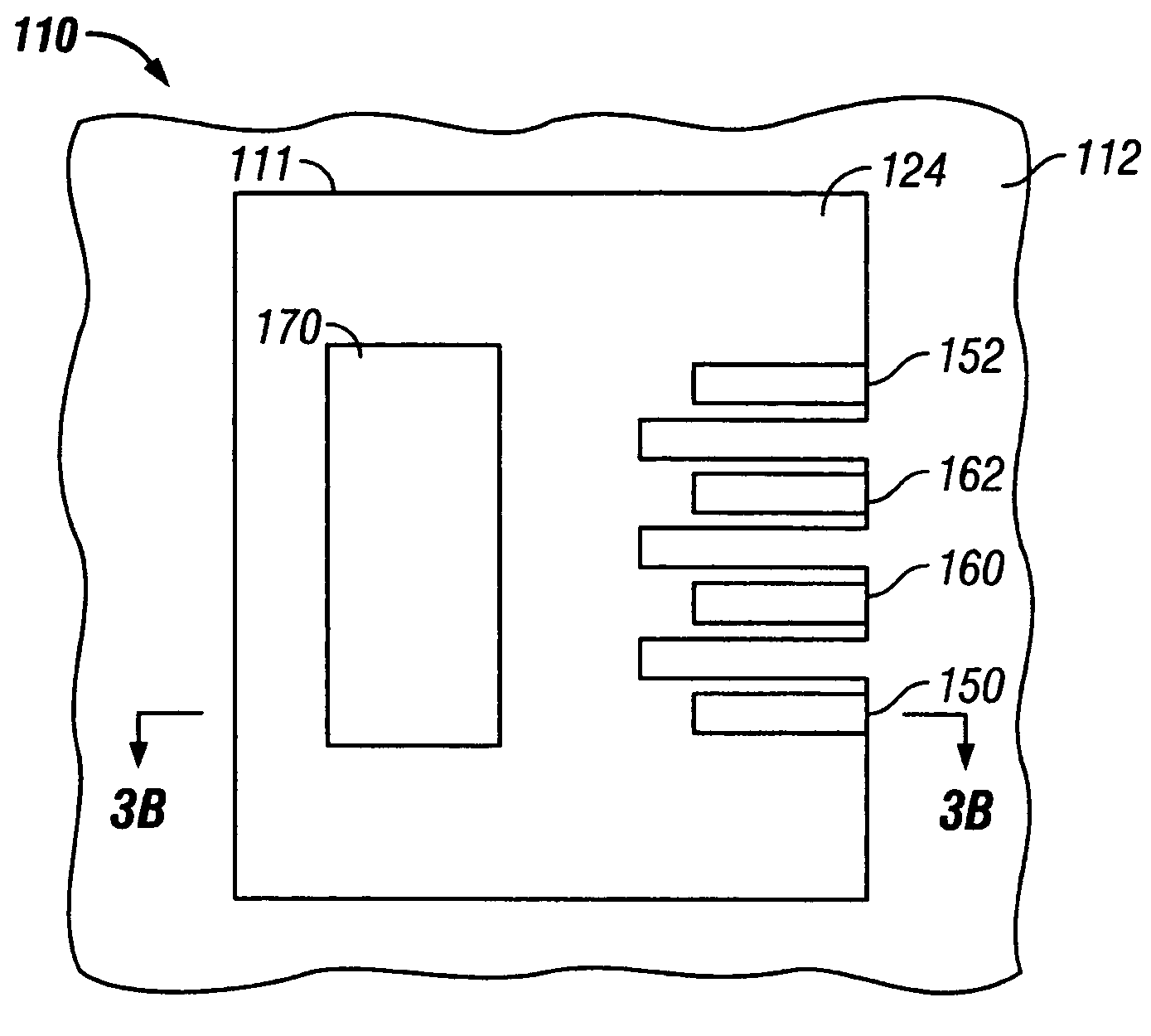
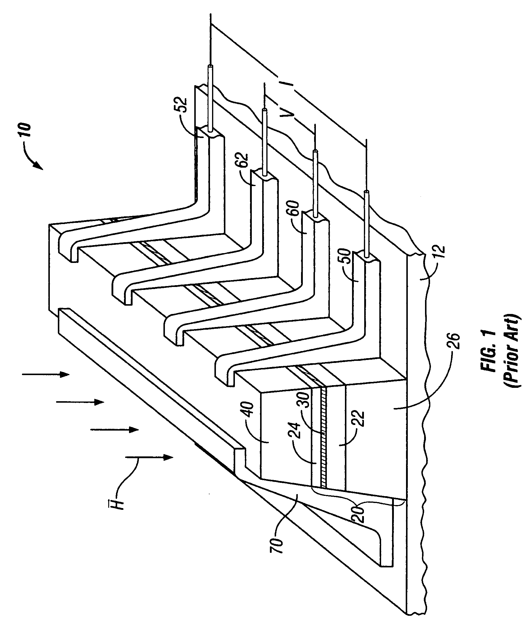
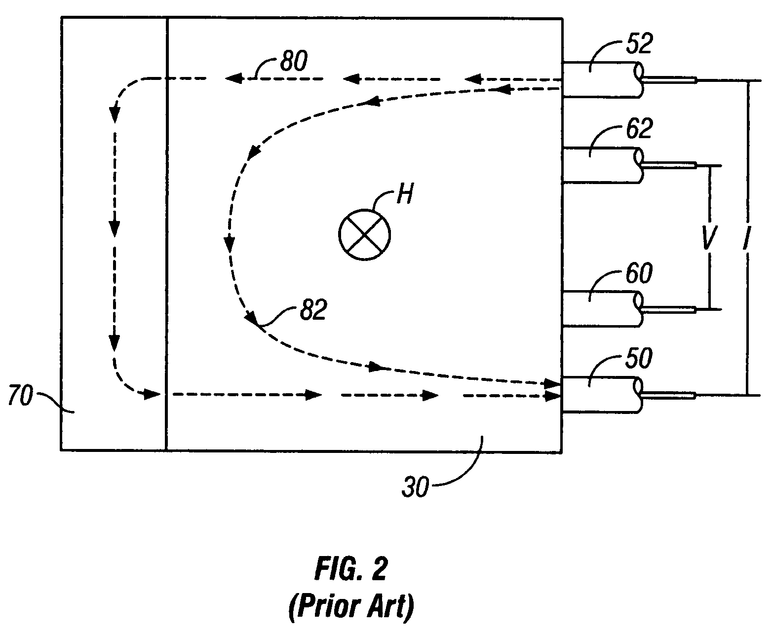
[0014]FIG. 1 is an isometric view of the prior art EMR sensor 10. The EMR sensor 10 includes a structure 20 that is a III–V heterostructure formed on a semiconducting substrate 12 such as GaAs. However, the EMR sensor described in this invention is not restricted to III–V semiconductor materials. For example, it may also be formed on the basis of silicon. The heterostructure 20 is a mesa above substrate 12 that results from a subtractive process, such as reactive-ion-etching (RIE). The heterostructure 20 includes a first layer 22 of semiconducting material having a first band-gap, a second layer 30 of semiconducting material formed on top of the first layer 22 and having a second band gap smaller than the first band gap, and a third layer 24 of semiconducting material formed on top of the second layer 30 and having a third band gap greater than the second band gap. The materials in first and third layers 22, 24 may be similar or identical. An energetic potential well (quant...


PUM

PropertyMeasurementUnit
thicknessaaaaaaaaaa
thicknessaaaaaaaaaa
thicknessaaaaaaaaaa

Abstract

An extraordinary magnetoresistance (EMR) sensor has a planar shunt and planar leads formed on top of the sensor and extending downward into the semiconductor active region, resulting. Electrically conductive material, such as Au or AuGe, is first deposited into lithographically defined windows on top of the sensor. After liftoff of the photoresist a rapid thermal annealing process causes the conductive material to diffuse downward into the semiconductor material and make electrical contact with the active region. The outline of the sensor is defined by reactive etching or other suitable etching techniques. Insulating backfilling material such as Al-oxide is deposited to protect the EMR sensor and the edges of the active region. Chemical mechanical polishing of the structure results in a planar sensor that does not have exposed active region edges.

Description

BACKGROUND OF THE INVENTION[0001]1. Field of the Invention[0002]This invention relates generally to a magnetoresistive sensor, and more particularly to such a sensor based on extraordinary magnetoresistance (EMR).[0003]2. Description of the Related Art[0004]A magnetoresistive sensor based on extraordinary magnetoresistance (EMR) has been proposed as a read-head sensor for magnetic recording hard disk drives. Because the active region in the EMR sensor is formed of nonmagnetic semiconductor materials, the EMR sensor does not suffer from the problem of magnetic noise that exists in read-head sensors based on giant magnetoresistance (GMR) and tunneling magnetoresistance (TMR), both of which use magnetic films in their active regions.[0005]The EMR sensor is fabricated as a mesa comprising a semiconductor heterostructure on a substrate. A pair of voltage leads and a pair of current leads are formed on one side of the mesa in contact with the semiconductor active region and an electricall...

Claims


Application Information

Patent Timeline
Patent Type & Authority Patents(United States)
IPC IPC(8): G11B5/39G01R27/08G01R33/02
CPCB82Y25/00G01R33/093G01R33/095
Inventor CHATTOPADHYAY, AMITAVAFONTANA, JR., ROBERT E.GURNEY, BRUCE A.MAAT, STEFANMARINERO, ERNESTO E.
Owner WESTERN DIGITAL TECH INC
Why Eureka
Try Eureka