Method and device for producing layout patterns of a semiconductor device having an even wafer surface

a technology of layout pattern and semiconductor device, which is applied in the direction of cad circuit design, total factory control, instruments, etc., can solve the problems of excessive different amount of abrasion of the wafer surface, and filling cells composed only of wells in vacant areas, so as to reduce the trouble of arithmetic processes

Inactive Publication Date: 2007-04-24
RENESAS ELECTRONICS CORP
View PDF24 Cites 7 Cited by
  • Summary
  • Abstract
  • Description
  • Claims
  • Application Information

AI Technical Summary

Benefits of technology

[0009]It is an object of the present invention to provide a method and device for producing the layout pattern of a semiconductor device that enables uniform planarization of the wafer surface in the CMP processing carried out before forming transistors, and further, that enables a reduction of trouble of the arithmetic processes when producing mask data.
[0010]In the present invention, in order to achieve the above-described objects, primitive cells, which are circuit patterns corresponding to each of the constituent elements of the semiconductor device, are arranged in the element formation area of the semiconductor device, and at least one fill cell with a diffusion layer and no wiring is arranged in a vacant area that is generated in the element formation area after all primitive cells have been arranged. Since the fill cells are arranged so as to make the data ratio of the diffusion layer (area ratio of the diffusion layer) falls within a prescribed range, uneven distribution of the diffusion layers is eliminated, whereby a wafer having a uniform surface can be obtained even when CMP is conducted to remove the insulating film on a wafer having diffusion layers and trenches formed thereon.
[0011]Further, fill cells in the present invention are arranged after primitive cells have been arranged and before mask data are made, and the arithmetic processes for making mask data can therefore be reduced.
[0012]In the present invention, a plurality of types of fill cells having different sizes are prepared and then arranged in vacant areas that are generated in the element formation area after all primitive cells have been arranged, this arrangement process proceeding in order of size, starting from the largest fill cells that can be arranged in vacant areas. These processes reduce trouble of the arrangement process of the fill cells. In addition, the above-described plurality of types of fill cells are each identified by identifiers having the same amount of information. This method prevents increase in the amount of calculation when making mask data from a layout pattern.
[0013]Finally, in the present invention, each of the constituent elements of a semiconductor device are grouped in advance so as to make constituent elements having related operations belong to the same group. Group information that indicates the type of groups is given to each constituent element in that group. Reference is made to this group information when producing the layout pattern of a semiconductor device, the primitive cells associated with constituent elements of the same groups are arranged in proximity. This makes it possible to shorten wiring between constituent elements, reduce the wiring capacitance, and obtain a semiconductor device that operates at higher speed.

Problems solved by technology

At this time, polishing proceeds further in regions of the wafer surface having few diffusion layers than in areas having many diffusion layers, raising the problem of excessive abrasion of the wafer surface.
In other words, there is the problem that the amount of abrasion of the wafer surface differs depending on the distribution of the diffusion layers.
These problems in processing the wafer surface accompany miniaturization of semiconductor devices.
Nevertheless, such an arrangement of fill cells composed only of wells in vacant areas cannot solve the above-described problems in processing the wafer surface.
However, a method in which dummy data are added to the mask data when making mask data is problematic because the distribution of diffusion layers and the size of vacant areas must be calculated from the layout pattern, and this calculation entails complex arithmetic processes and an excessive amount of processing time.
However, since the problem addressed by Patent Document 1 is the distribution of wiring such as gate electrodes as described above, there is no disclosure regarding the significance of the distribution of diffusion layers in Patent Document 1.

Method used


Image

  • Method and device for producing layout patterns of a semiconductor device having an even wafer surface
  • Method and device for producing layout patterns of a semiconductor device having an even wafer surface
  • Method and device for producing layout patterns of a semiconductor device having an even wafer surface

Examples


Embodiment Construction

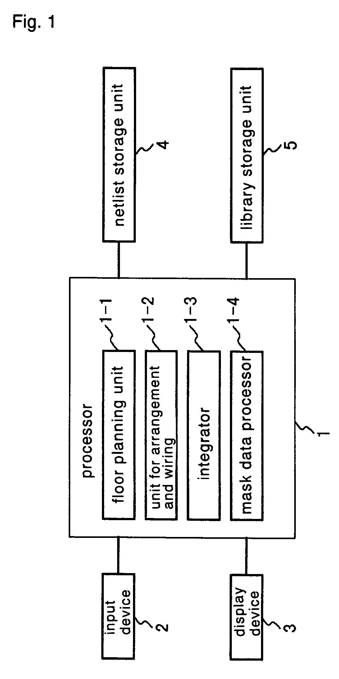
[0024]As shown in FIG. 1, the device and for producing a layout pattern of the present invention comprises processor 1, input device 2, display device 3, netlist storage unit 4, and library storage unit 5.

[0025]Processor 1 comprises floor planning unit 1-1, unit for arrangement and wiring 1-2, integrator 1-3, and mask data processor 1-4. Processor 1 may consist of, for example, a computer that, in accordance with a program, executes processing for producing the layout pattern of the present invention described hereinbelow.

[0026]Processor 1 executes processing in accordance with a program that has been provided in advance, by commands supplied from input device 2 or the like, and the results of this processing are indicated by display device 3. In addition, processor 1 refers, as necessary, to data stored in netlist storage unit 4 and library storage unit 5.

[0027]Input device 2 is used for supplying data and commands as input to processor 1.

[0028]Display device 3 is controlled by pro...


PUM


Abstract

Primitive cells, which are circuit patterns of the constituent elements of a semiconductor device, are arranged in the element formation area of a semiconductor device, and at least one fill cell with a diffusion layer and no wiring, is arranged in the vacant areas that are generated in the element formation area after the primitive cells have been arranged.

Description

BACKGROUND OF THE INVENTION[0001]1. Field of the Invention[0002]The present invention relates to a method and device for producing a layout pattern of a semiconductor device.[0003]2. Description of the Related Art[0004]Recent fabrication methods of semiconductor devices are described below. First, wells are formed close to the wafer surface and impurities are injected into the wells to form diffusion layers. Thereafter trenches are formed in element isolation areas for isolating each element. An oxide film (insulating film) is then formed by a well-known CVD (Chemical Vapor Deposition) method over the entire surface of the wafer including the interiors of the trenches. The surface of the formed oxide film is uneven, that is, is higher at the diffusion layers and lower at the trenches. A known CMP (Chemical Mechanical Polishing) method is then carried out to planarize the wafer surface, so that the oxide film of the wafer surface is removed to expose the surface of the diffusion laye...

Claims


Application Information

Patent Timeline
Patent Type & Authority Patents(United States)
IPC IPC(8): H01L21/82G06F17/50G06F15/00H01L21/822H01L27/02H01L27/04
CPCG06F17/5068H01L27/0203G06F2217/12G06F2119/18G06F30/39Y02P90/02
Inventor KAWASHIMA, HIDEKAZUKATOH, TETSUYA
Owner RENESAS ELECTRONICS CORP
Why Eureka
Try Eureka