Low drift planar waveguide grating sensor and method for manufacturing same

a technology sensor, which is applied in the field of planar waveguide grating (pwg) sensors, can solve the problems of high yield and low cost of disposable pwg sensors, performance of these disposable pwg sensors, and difficulty in balancing cost and performance in making a disposable pwg

Inactive Publication Date: 2007-05-15
CORNING INC
View PDF28 Cites 3 Cited by
  • Summary
  • Abstract
  • Description
  • Claims
  • Application Information

AI Technical Summary

Problems solved by technology

However, there are problems associated with manufacturing disposable PWG sensors 100 at a high yield and a low cost.
And, there are problems associated with the performance of these disposable PWG sensors 100.
The prior art demonstrates that there has been a struggle to balance the cost and performance in making a disposable PWG sensor 100.
However, the PWG sensor 100 which has a polymeric substrate 102 can suffer from a problematical optical signal loss that is due to absorption in the polymeric substrate 102.
Referring back to FIG. 1, it can be difficult to manufacture the PWG sensor 100 which has a polymeric substrate 102.
In particular, there is a significant manufacturing challenge in keeping the polymeric substrate 102 flat to ensure a uniform coupling angle for the light 116 that is directed into and reflected out-off the PWG sensor 100.
However, the use of a photolithography patterning and etching process to form a smooth and accurately reproduced diffraction grating 104 on the top surface of the glass substrate 102 can be challenging.
Unfortunately, this type of photolithography patterning process can be costly and as such it is not be suitable to manufa

Method used


Image

  • Low drift planar waveguide grating sensor and method for manufacturing same
  • Low drift planar waveguide grating sensor and method for manufacturing same
  • Low drift planar waveguide grating sensor and method for manufacturing same

Examples


example b

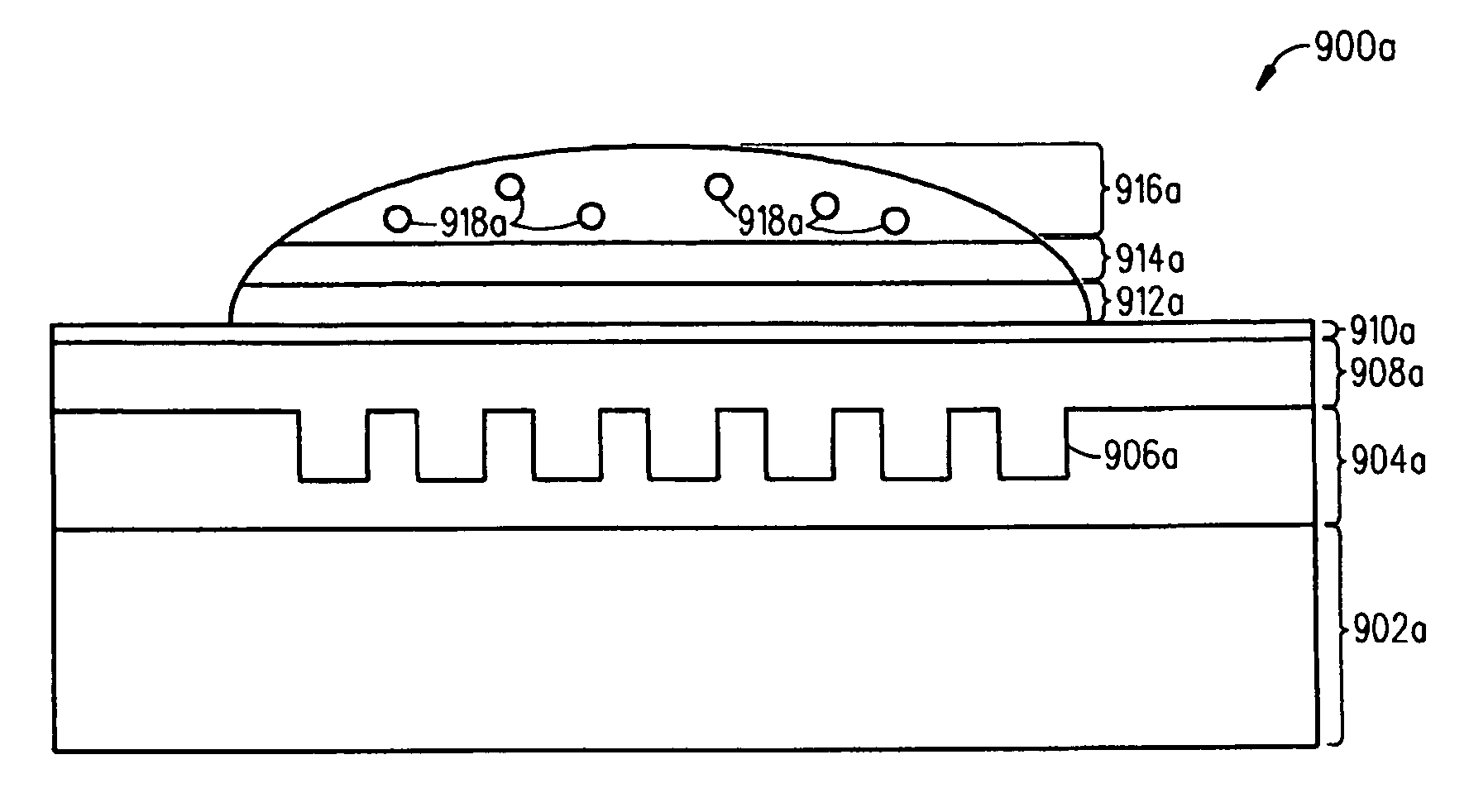
[0110] Another experiment was conducted so the assay performance of Fl-biotin interacting with immobilized Streptavidin could be compared by using 384 well microplates which had either inorganic PWG sensors 900b or prior art PWG sensors 500 incorporated therein.

[0111]The inorganic PWG sensor 900b array was fabricated by depositing onto a glass substrate 902b a 200 nm FSG cladding layer 904b which had a refractive index of 1.41 at 830 nm by PECVD. Then, grating patterns 906b were formed in the FSG cladding layer 904b by exposing a photoresist with a deep UV stepper, and 45 nm deep diffraction gratings 906b were etched into the FSG cladding layer 904b by using a RIE process and fluorocarbon gas CHF3. Then, a ˜148 nm thick Si-rich silicon nitride monomode waveguide 908b with a refractive index of 2.5 at 830 nm was deposited by PECVD over the diffraction gratings 904b. The prior art PWG sensor 500 array was fabricated by forming diffraction gratings 504 in a UV cured polymer layer 505 l...

example c

[0117] This experiment was conducted to examine if the origin of the higher assay signal for the inorganic PWG sensors 900a and 900b was due to the higher index contrast of the waveguide structure, or to the surface interaction between the waveguide structure, the surface chemistry layer 912a and 912b, and the solution containing the molecules 914a and 914b of interest. Eight microplates of either inorganic PWG sensors 900a or 900b as described above with respect to FIGS. 9A and 9B but with different waveguides and surface layers where tested and the Fl-biotin to Streptavidin assay results compared. The waveguide materials compared were the Nb2O5 waveguides (PWG sensor 900a) as was typically used in prior art example PWG sensor 500, and silicon rich silicon nitride (PWG sensor 900b). The surface layers compared were SiO2 surface as was typically used in prior art example PWG sensor 500, and silicon rich silicon nitride surface layers described in PWG sensors 900a and 900b. Both sili...


PUM


Abstract

A planar waveguide grating (PWG) sensor is described herein which exhibits a low signal drift and an enhanced sensitivity due to the use of a fully dense silicon-rich nitride surface layer. In the preferred embodiment, the silicon rich silicon nitride surface layer has a composition which includes Si and N, and optionally H, Ge and/or O, where a Si/N atomic ratio is greater than 0.75. In addition, the silicon rich nitride surface layer has a refractive index that is greater than 2.45 and less than 3.2 at a wavelength of operation. A method is also described herein for manufacturing the PWG sensor with acceptable costs and high yields by utilizing well known semiconductor processes and tools.

Description

BACKGROUND OF THE INVENTION[0001]1. Field of the Invention[0002]The present invention relates to a planar waveguide grating (PWG) sensor which exhibits a low signal drift and an enhanced sensitivity due to the use of a fully dense silicon rich silicon nitride surface layer. In addition, the present invention relates to a method for manufacturing the PWG sensor with acceptable costs and high yields by utilizing well known semiconductor processes and tools.[0003]2. Description of Related Art[0004]The following abbreviations are herewith defined, at least some of which are referred to in the ensuing description of the prior art and the preferred embodiments of the present invention.[0005]APCVDAtmospheric Pressure Chemical Vapor DepositionCVDChemical Vapor DepositionFIBFocused Ion BeamFSGFluorine Doped Silica GlassLPCVDLow Pressure Chemical Vapor DepositionPECVDPlasma Enhanced Chemical Vapor DepositionPWGPlanar Waveguide GratingPVDPhysical Vapor DepositionRIEReactive Ion EtchingSACVDSub...

Claims


Application Information

Patent Timeline
IPC IPC(8): G02B6/00G02B6/10G02B6/34
CPCB01L3/5085G01N21/253G01N21/7743G01N33/54373G02B5/1809G02B6/12007G02B6/1221G02B6/13B01L2300/0654B01L2300/0829
Inventor BELLMAN, ROBERT A.WANG, CHUAN-CHE
Owner CORNING INC
Why Eureka
Try Eureka