Single crystalline aluminum nitride film, method of forming the same, base substrate for group III element nitride film, light emitting device and surface acoustic wave device

a technology of aluminum nitride and aluminum nitride, which is applied in the direction of polycrystalline material growth, chemically reactive gas growth, crystal growth process, etc., can solve the problems of large distortion at the junction interface between the sapphire substrate and the thin aln film, and it is still extremely difficult to obtain a group iii element nitride thin film having few defects, and achieve excellent crystallinity , low dislocation density, and high luminous efficiency

Inactive Publication Date: 2007-05-22
TOKYO INST OF TECH
View PDF7 Cites 12 Cited by
  • Summary
  • Abstract
  • Description
  • Claims
  • Application Information

AI Technical Summary

Benefits of technology

[0010]It is an object of the present invention which has been made in view of the above problems to provide a single crystalline aluminum nitride film which has a low dislocation density, little lattice mismatching and excellent crystallinity and can ensure the formation of a Group III element nitride film excellent in luminous efficiency, a method of forming the same, a base substrate for a Group III element nitride film, a light emitting device and a surface acoustic wave device.
[0020]In the present invention, an aluminum oxynitride (alon) layer is formed on the surface of a single crystalline α-Al2O3 substrate, for example, a sapphire substrate and a single crystalline aluminum nitride (AlN) film is formed on this alon layer by nitriding the substrate. Therefore, the obtained single crystalline AlN film has an extremely low dislocation density and excellent crystallinity. Accordingly, when this single crystalline AlN film is used as a light emitting device, an ultraviolet light emitting device having extremely high luminous efficiency can be obtained and can be used in a high-density optical memory and also in a wide variety of fields as an ultraviolet light receiving device. Further, when a group III element nitride semiconductor typified by a GaN-based semiconductor is epitaxially grown on this single crystalline AlN film having excellent crystallinity, a group III element nitride semiconductor single crystalline film having extremely high crystallinity and few defects can be formed. Therefore, a blue light emitting device or ultraviolet light emitting device comprising this group IIII element nitride semiconductor single crystalline film has greatly improved luminous efficiency. Further, since single crystalline AlN can be used in a surface acoustic wave device and a single crystalline AlN film having excellent crystallinity is obtained by the present invention, the drive efficiency of a surface acoustic wave device comprising this film can be enhanced.

Problems solved by technology

Due to its great lattice mismatching with the material of the substrate, it is still extremely difficult to obtain a group III element nitride thin film having few defects.
However, since the buffer layer of AlN or the like also has great lattice mismatching with the sapphire substrate, it is difficult to obtain a defect-free homogeneous thin film.
In all of the above methods, large distortion remains at the junction interface between the sapphire substrate and the thin AlN film due to great lattice mismatching therebetween.
This is the main factor that lowers the luminous efficiency of a light emitting device.
As a result, the conventional blue LED has a low luminous efficiency of 22% and the conventional ultraviolet LED has a low luminous efficiency of only 7.5%.
However, as this prior art technique uses a bulky apparatus for MOVPE, MBE or the like to form an aluminum oxynitride layer and forms a GaN film on the aluminum oxynitride layer, it cannot be said that lattice mismatching has been improved sufficiently.

Method used


Image

  • Single crystalline aluminum nitride film, method of forming the same, base substrate for group III element nitride film, light emitting device and surface acoustic wave device
  • Single crystalline aluminum nitride film, method of forming the same, base substrate for group III element nitride film, light emitting device and surface acoustic wave device
  • Single crystalline aluminum nitride film, method of forming the same, base substrate for group III element nitride film, light emitting device and surface acoustic wave device

Examples


example 1

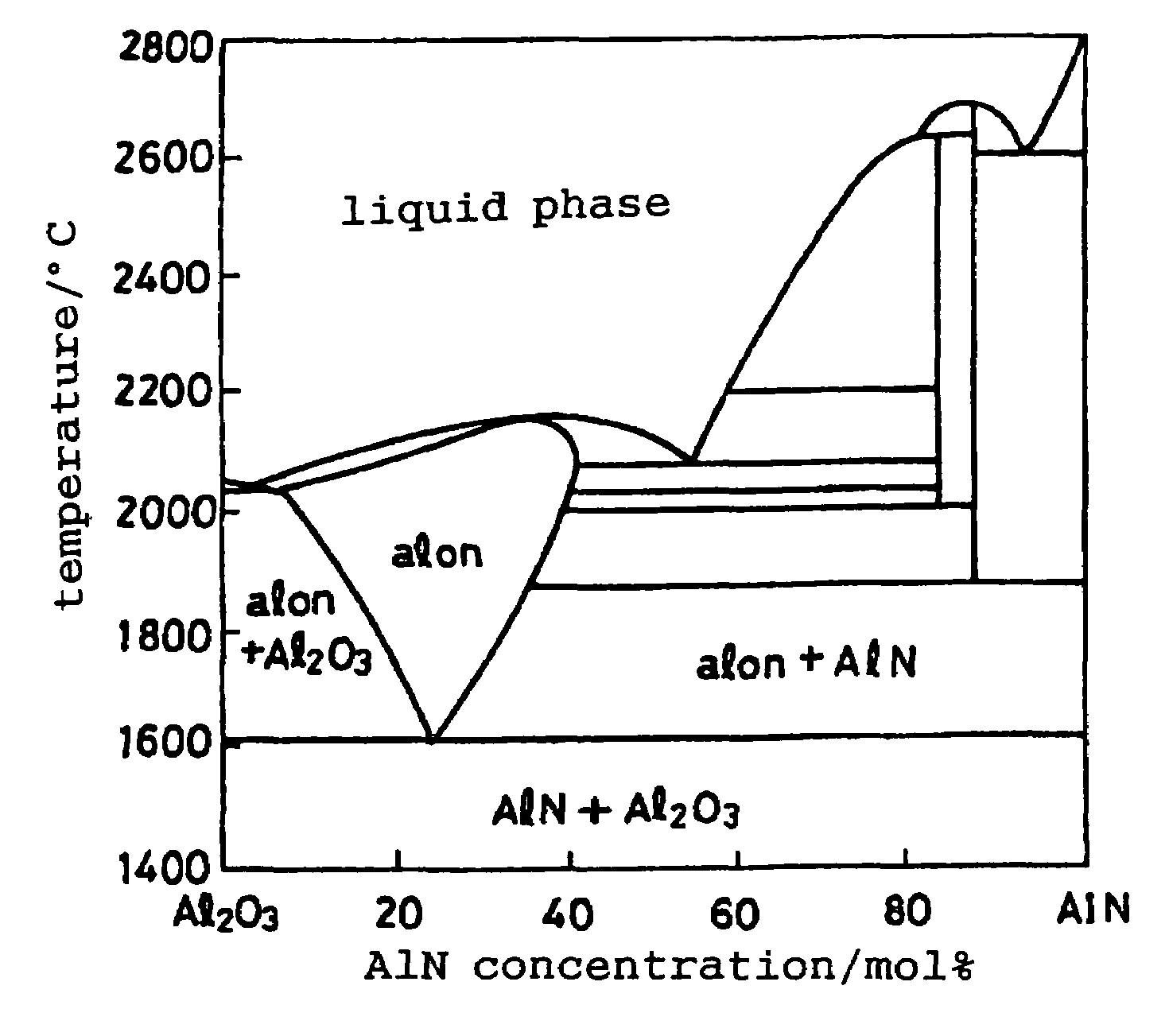
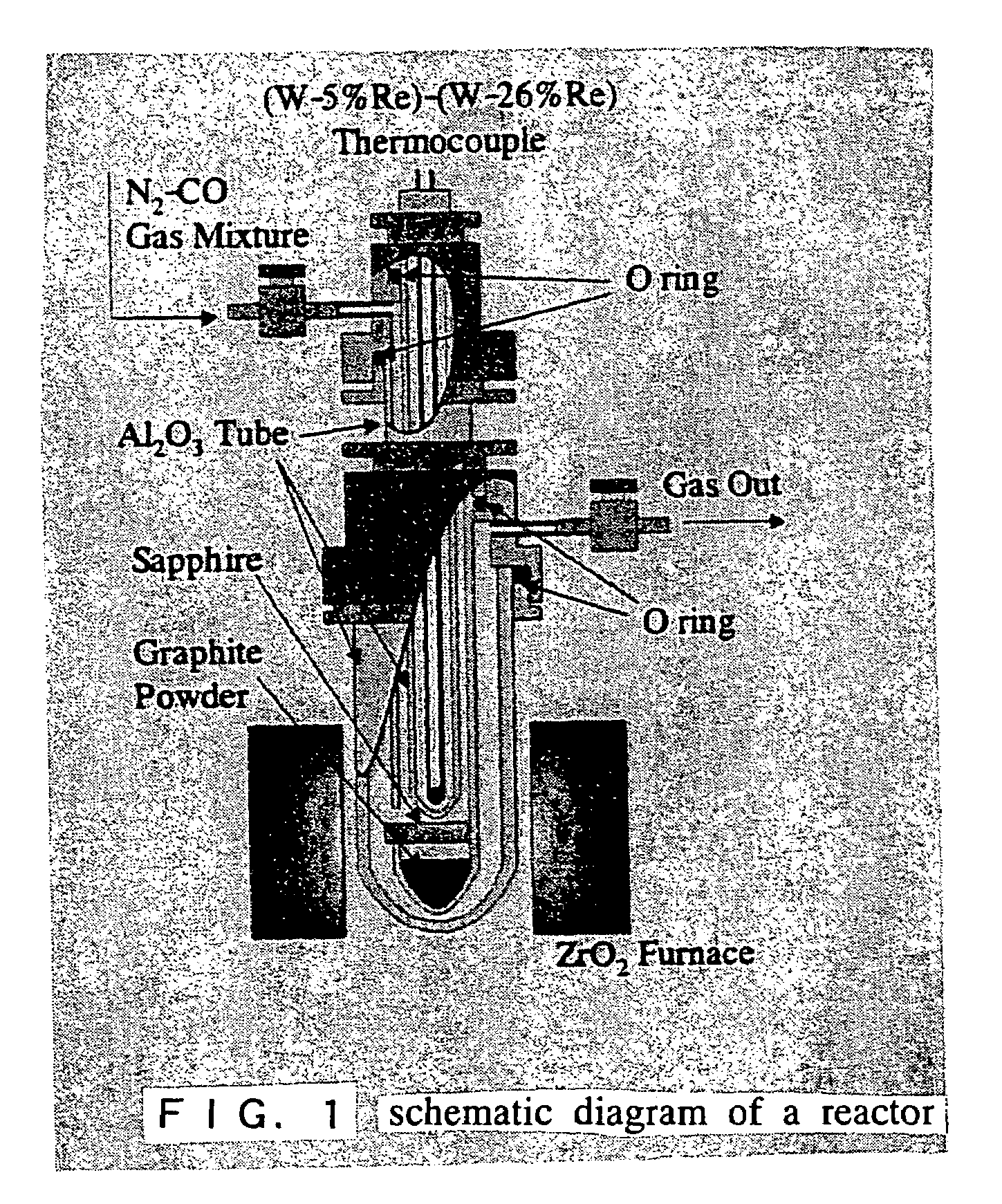
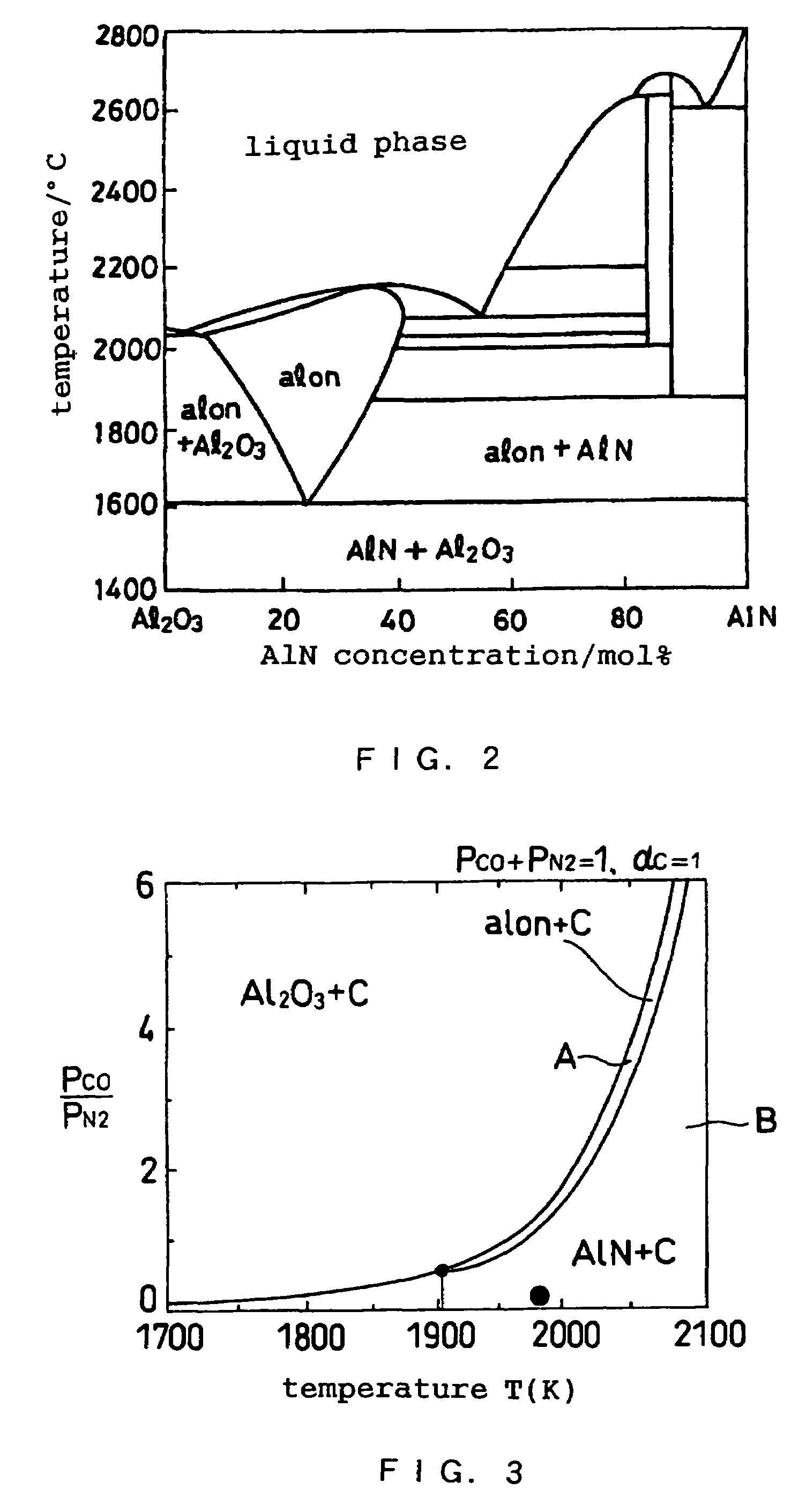
[0068]AlN and alon phases were formed from an N2-CO mixed gas and graphite at 1,973K by nitriding a sapphire substrate using a reactor shown in FIG. 1. The sapphire substrate (10 mm×10 mm×1 mm) whose surface had A crystal face (11-20) and graphite powders (purity of 99.999%) were placed at the bottom of an Al2O3 reaction tube. The inside of the reaction tube was completely evacuated and dehydrated by a rotary pump in advance and completely substituted by a mixed gas having a ratio of the carbon monoxide (CO) partial pressure to the nitrogen (N2) partial pressure of 0.1. Thereafter, this mixed gas was caused to flow at a fixed rate of 55 ml / min. The total inside pressure of the reactor was 1 atmospheric pressure. The bottom of the reaction tube was inserted into the equalizing portion of a furnace to quickly heat the sample and maintain it at 1,973K so as to start a reaction. After the sample was kept for 24 hours, the reaction tube was pulled out from the furnace to quench the sampl...

example 2

[0074]AlN and alon phases were formed from an N2-CO mixed gas and graphite at 1,973K by nitriding a sapphire substrate using the experimental device shown in FIG. 1. The sapphire substrate (10 mm×10 mm×1 mm) whose surface had C crystal face and graphite powders (purity of 99.999%) were placed at the bottom of an Al2O3 reaction tube. The inside of the reaction tube was completely evacuated and dehydrated by a rotary pump in advance and completely substituted by a CO—N2 mixed gas having a PCO / PN2 ratio of 0.1. Thereafter, this mixed gas was caused to flow at a fixed rate of 55 ml / min. The total inside pressure of the reactor was 1 atmospheric pressure. The bottom of the reaction tube was inserted into the equalizing portion of a furnace to quickly heat the sample and maintain it at 1,973K so as to start a reaction. After the sample was kept for 24 hours, the reaction tube was pulled out from the furnace to quench the sample, thus completing the reaction.

[0075]The pole figure of the Al...


PUM

PropertyMeasurementUnit
weight ratioaaaaaaaaaa
thicknessaaaaaaaaaa
diameteraaaaaaaaaa

Abstract

A single crystalline aluminum nitride laminated substrate comprising a single crystalline α-Al2O3 substrate such as a sapphire substrate, an aluminum oxynitride layer formed on the substrate and a single crystalline aluminum nitride film as the outermost layer, wherein the dislocation density in the single crystalline aluminum nitride is 108 / cm2 or less.The above single crystalline aluminum nitride laminated substrate is formed by nitriding the substrate by heating in the presence of carbon, nitrogen and carbon monoxide.The above single crystalline aluminum nitride film has a law dislocation density, little lattice mismatching and excellent crystallinity. A Group III element nitride film having excellent luminous efficiency can be formed on this aluminum nitride film. The above laminated substrate is used in a base substrate for a Group III element nitride film, a light emitting device and a surface acoustic wave device.

Description

CROSS REFERENCE TO RELATED APPLICATION[0001]This application is a divisional of U.S. Ser. No. 10 / 247,539, filed Sep. 20, 2002, now U.S. Pat. No. 6,744,076, the entire contents of which are herein incorporated by reference and for which priority is claimed under 35 U.S.C. § 120; and this application claims priority under 35 U.S.C § 119(a) on Patent Application No. JP 2002-070229 filed in Japan on Mar. 14, 2002, the contents of which are herein incorporated by reference.DETAILED DESCRIPTION OF THE INVENTION[0002]1. Field of the Invention[0003]The present invention relates to a single crystalline aluminum nitride (AlN) film, a method of forming the same, which can ensure highly efficient formation of an aluminum nitride film, a base substrate for a Group III element nitride film, a light emitting device and a surface acoustic wave device.[0004]2. Description of the Prior Art[0005]Special attention has recently been paid to group III element nitride semiconductors typified by a gallium ...

Claims


Application Information

Patent Timeline
Patent Type & Authority Patents(United States)
IPC IPC(8): C30B25/00C30B25/02H01L21/20H01L33/32
CPCC30B25/02C30B29/403C30B29/406H01L21/0242H01L21/02433H01L21/02458H01L21/02488H01L21/02502H01L21/0254H01L21/02658H01L33/32
Inventor FUKUYAMA, HIROYUKINAGATA, KAZUHIRONAKAO, WATARU
Owner TOKYO INST OF TECH
Why Eureka
Try Eureka