Method for producing gate stack sidewall spacers

a sidewall spacer and gate stack technology, applied in the direction of chairs, semiconductor devices, stools, etc., can solve the problems of large thermal cycle of the gate device, material lack of the necessary structural integrity to survive subsequent processing steps, and excessive signal crosstalk between adjacent interconnection lines, etc., to achieve the effect of enhancing chemical vapor deposition

Active Publication Date: 2007-08-07
APPLIED MATERIALS INC
View PDF40 Cites 248 Cited by
  • Summary
  • Abstract
  • Description
  • Claims
  • Application Information

AI Technical Summary

Problems solved by technology

If the sidewall spacer is then fabricated from a relatively high k (k>7) material, such as silicon nitride, excessive signal crosstalk between adjacent interconnection lines can occur during use of the device containing the completed gate electrode.
While ultra-low k materials (k<3) may be employed as a spacer layer, these materials often lack the necessary structural integrity to survive subsequent processing steps and / or requisite oxygen and moisture imperviousness to protect the gate metal from corrosion.
In addition, conventional thermal chemical vapor deposition (CVD) process used to prepare silicon nitride spacer requires high deposition temperature, which is typically greater than 600° C. The nitride spacer deposited at high temperature has very good conformality (e.g. ≧95%); however, the high deposition temperature results in large thermal cycle for the gate device and is not compatible with advanced device manufacturing for 0.09 micron technology and beyond.

Method used


Image

  • Method for producing gate stack sidewall spacers
  • Method for producing gate stack sidewall spacers
  • Method for producing gate stack sidewall spacers

Examples


Embodiment Construction

[0016]The present invention encompasses forming sidewall spacers for gate stacks by applying a silicon-based film to a gate structure. In some embodiments, a spacer layer is formed by deposition of silicon carbide, oxygen doped silicon carbide, nitrogen doped silicon carbide, or carbon doped silicon nitride adjacent a gate dielectric. In another embodiment, the spacer layer is formed by deposition of carbon doped silicon oxynitride.

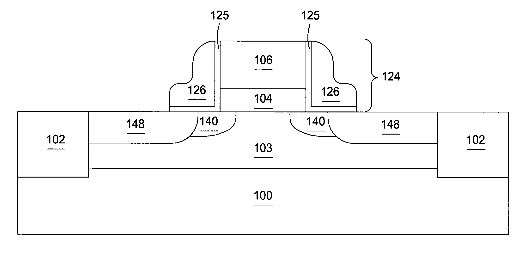
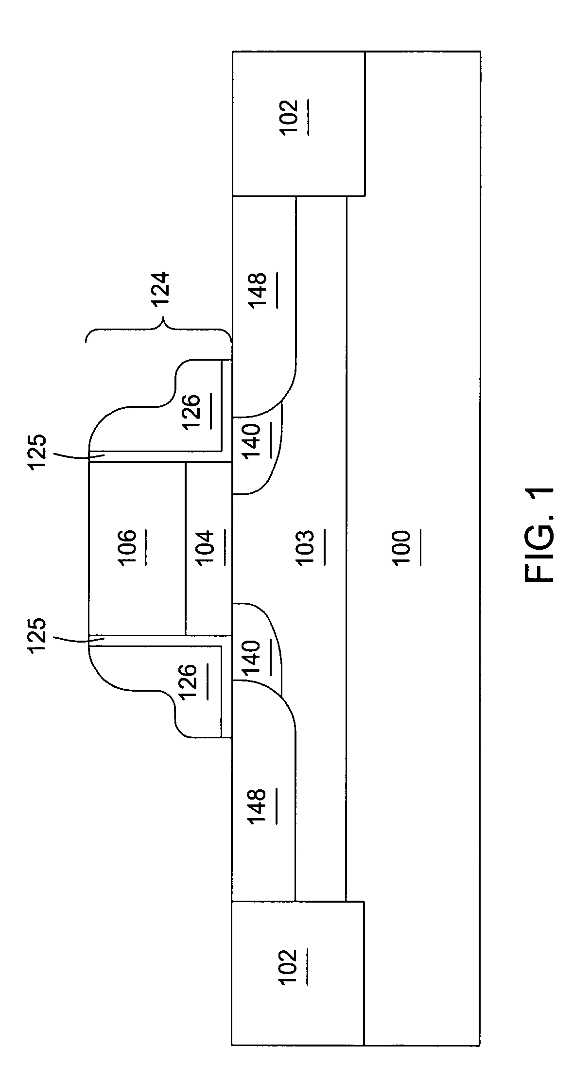
[0017]FIG. 1 illustrates a transistor having a gate structure formed according to one embodiment of the invention. Referring to FIG. 1, a plurality of field isolation regions 102 are formed in a substrate 100 (e.g., a silicon wafer). The plurality of field isolation regions 102 isolate a well 103 of one type conductivity (e.g., p-type) from adjacent wells (not shown) of other type conductivity (e.g., n-type). Then, a gate dielectric layer 104 is formed on the substrate 100 and on isolation regions 102. Typically, gate dielectric layer 104 may be formed by...


PUM

PropertyMeasurementUnit
dielectric constantaaaaaaaaaa
temperatureaaaaaaaaaa

Abstract

A method for forming sidewall spacers on a gate stack by depositing one or more layers of silicon containing materials using PECVD process(es) on a gate structure to produce a spacer having an overall k value of about 3.0 to about 5.0. The silicon containing materials may be silicon carbide, oxygen doped silicon carbide, nitrogen doped silicon carbide, carbon doped silicon nitride, nitrogen doped silicon oxycarbide, or combinations thereof. The deposition is performed in a plasma enhanced chemical vapor deposition chamber and the deposition temperature is less than 450° C. The sidewall spacers so produced provide good capacity resistance, as well as excellent structural stability and hermeticity.

Description

BACKGROUND OF THE INVENTION[0001]1. Field of the Invention[0002]Embodiments of the present invention generally relate to a method for producing sidewall spacers for gate stacks on semiconductor substrates.[0003]2. Description of the Related Art[0004]Ultra-large-scale integrated (ULSI) circuits typically include more than one million transistors that are formed on a semiconductor substrate and which cooperate to perform various functions within an electronic device. Such transistors may include complementary metal-oxide-semiconductor (CMOS) field effect transistors.[0005]A CMOS transistor includes a gate structure that is disposed between a source region and a drain region defined in the semiconductor substrate. The gate structure (stack) generally comprises a gate electrode formed on a gate dielectric material. The gate electrode controls a flow of charge carriers, beneath the gate dielectric, in a channel region that is formed between the drain region and the source region, so as t...

Claims


Application Information

Patent Timeline
Patent Type & Authority Patents(United States)
IPC IPC(8): H01L21/31H01L21/469
CPCH01L21/02126H01L21/02167H01L21/0217H01L21/02211H01L21/02274H01L21/02329H01L21/0234H01L21/3148H01L21/31633H01L21/3185H01L29/4983H01L29/6659A47C4/04A47C7/402A47C7/405A47C7/626
Inventor ARGHAVANI, REZAKWAN, MICHAEL CHIUXIA, LI-QUNYIM, KANG SUB
Owner APPLIED MATERIALS INC
Why Eureka
Try Eureka