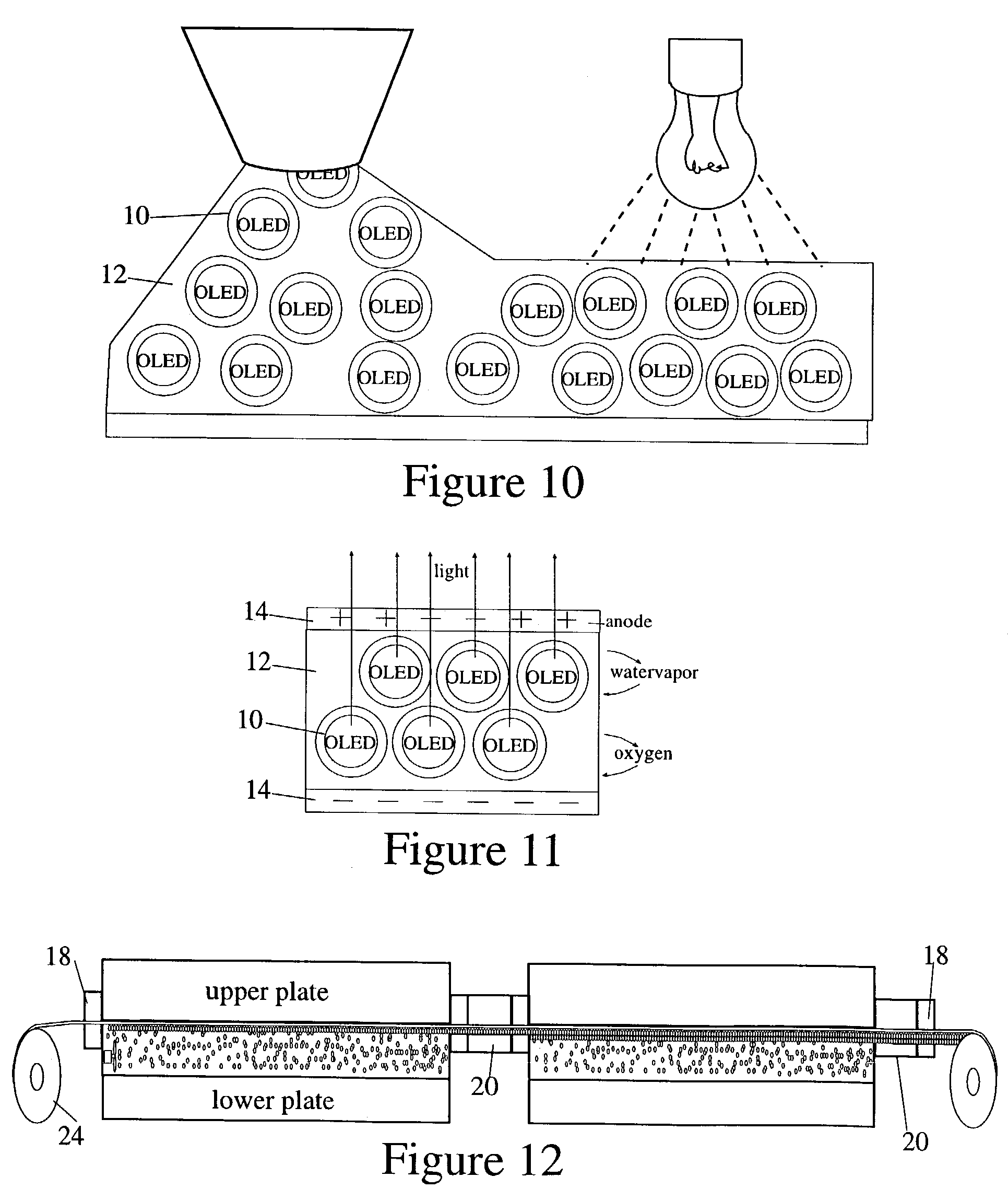
[0022]It is an object of the present invention to overcome the drawbacks of the prior art. It is an object of the present invention to provide a method of fabricating a light active device by dispersing three dimensionally a semiconductor particulate within a carrier material. The resulting structure has individual point sources of
light emission dispersed with a
protective barrier material. The barrier material provides strength to the device and adhesion to the electrodes and / or other films and prevents
contamination of the semiconductor particulate. The inventive fabrication method also allows multiple colors to be emitted from the inventive mixture between a
single pair of electrodes forming a pixel or device. In an inventive display driving scheme, an array of such pixels is driven so that bursts of color emissions occurs in rapid succession resulting in the
perception by the
human eye of a range of colors in the
visible spectrum. Thus, in accordance with this aspect of the invention, a single emissive layer and pair of electrodes can be used to create a
full color video display. The inventive OLAM™ structure can also be used to detect a spectrum of colors when the device is constructed as a
photodetector.
[0028]The organic light
active layer may also include third emitting particles including a third electroluminescent conjugated polymer. The third emitting particles emit a number of photons of a third color and / or intensity in response to a third turn-on
voltage applied to the electrodes and a different number of photons of the third color and / or intensity in response to other turn-on voltages. A
full color display can be obtained by incorporating an array of pixels each capable of emitting different colors, such as a first color red, a second color green and a third color blue. The color emitters can be a mix of organic and
inorganic materials. For example, an organic conjugated polymer emitter can be used as a red emitter and an inorganic
rare earth metal or
metal alloy, or doped inorganic semiconductor, can be used as a green emitter. This combination of organic and inorganic emitters may expand the potential candidates for emissive materials enabling the inventive device to be tuned for specific applications.
[0037]As is described further herein, the microcapsule composition may be effective for enabling a “
self healing” capability of the fabricated OLED device. In this case, the microcapsule includes a composition that causes the microcapsule to rupture if electrical energy above a threshold is applied to the microcapsule. For example, if a particular microcapsule is aligned so the during use of the OLED device it becomes a short between the electrodes, or if the microcapsule is adjacent to a dust particle or other foreign inclusion, creating such a short, when a
electric potential is applied between the electrodes energy exceeding a predetermined threshold will pass through the microcapsule causing the
capsule to rupture and disconnect the short. By this construction, the microcapsule is automatically removed from the path of conduction of electrical energy in the event of a short.
[0038]In accordance with another aspect of the invention, the microcapsule shell and / or
internal phase may include a composition effective to provide a barrier against degradation of the OLED material. The OLED microcapsules are dispersed within a
carrier fluid. This
carrier fluid also provides a barrier against the intrusion of substances which degrade the OLED material.
[0041]The typical OLED includes an OLED component that is a hole transport material and an OLED component that is an electron transport material. In accordance with a formulation of the inventive microcapsules, the shell comprises an OLED component material that is either the hole transport material or the electron transport material, and the
internal phase of the microcapsule includes the OLED component material that is the other of the hole transport material and the electron transport material. Depending on the desired optical qualities of the fabricated OLED device, the carrier material can be selected so that it has optical properties during use of the OLED device that are transparent, diffusive, absorptive, and / or reflective to
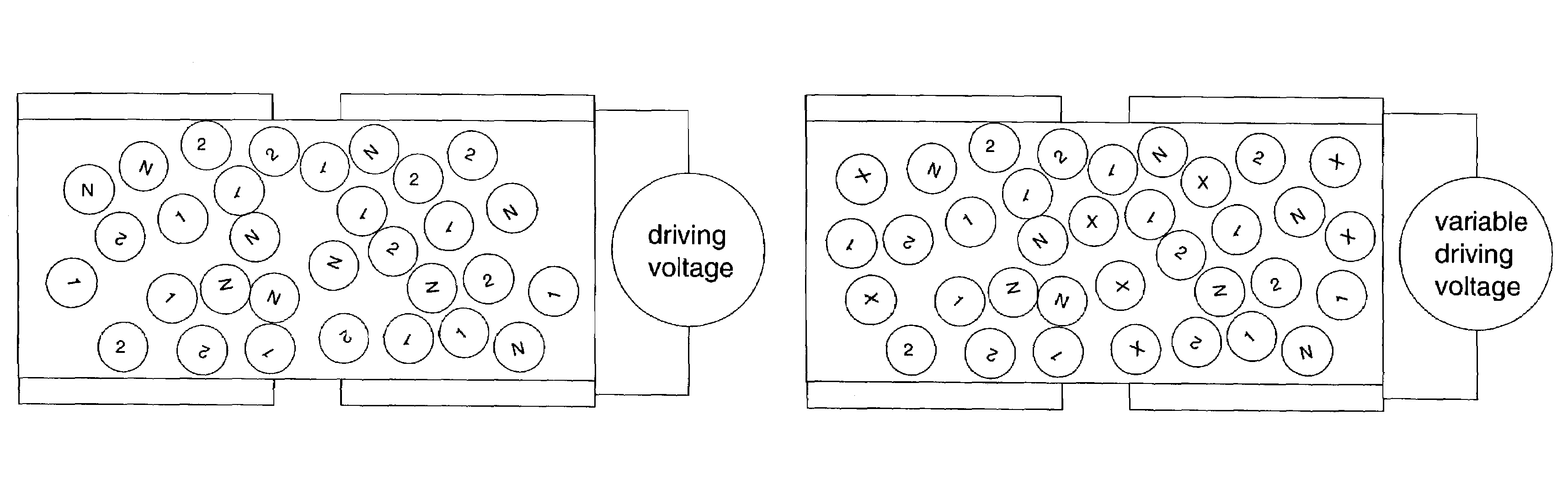
light energy. The composition of the OLED particulate can be selected so that the electrical characteristics of the OLED particulate includes, an electro or
magneto rheological characteristic. This rheological characteristic is effective for causing the OLED particulate to move within the carrier and orient in response to an applied electrical or
magnetic field.

