

Potassium niobate deposited body and method for manufacturing the same, surface acoustic wave device, frequency filter, oscillator, electronic circuit, and electronic apparatus
a technology of potassium niobate and deposited bodies, which is applied in the direction of niobium compounds, piezoelectric/electrostrictive transducers, generators/motors, etc., can solve the problems high acoustic velocity, and inability to meet the requirements of high electromechanical coupling coefficient,
- Summary
- Abstract
- Description
- Claims
- Application Information
AI Technical Summary
Benefits of technology
Problems solved by technology
Method used
Image

Examples
first embodiment
1. First Embodiment
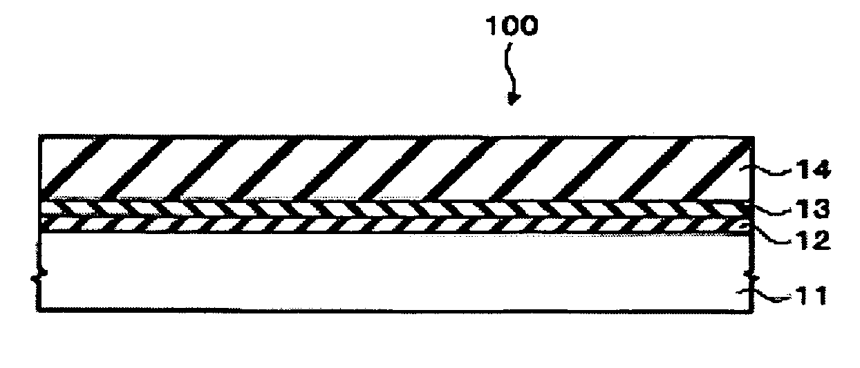
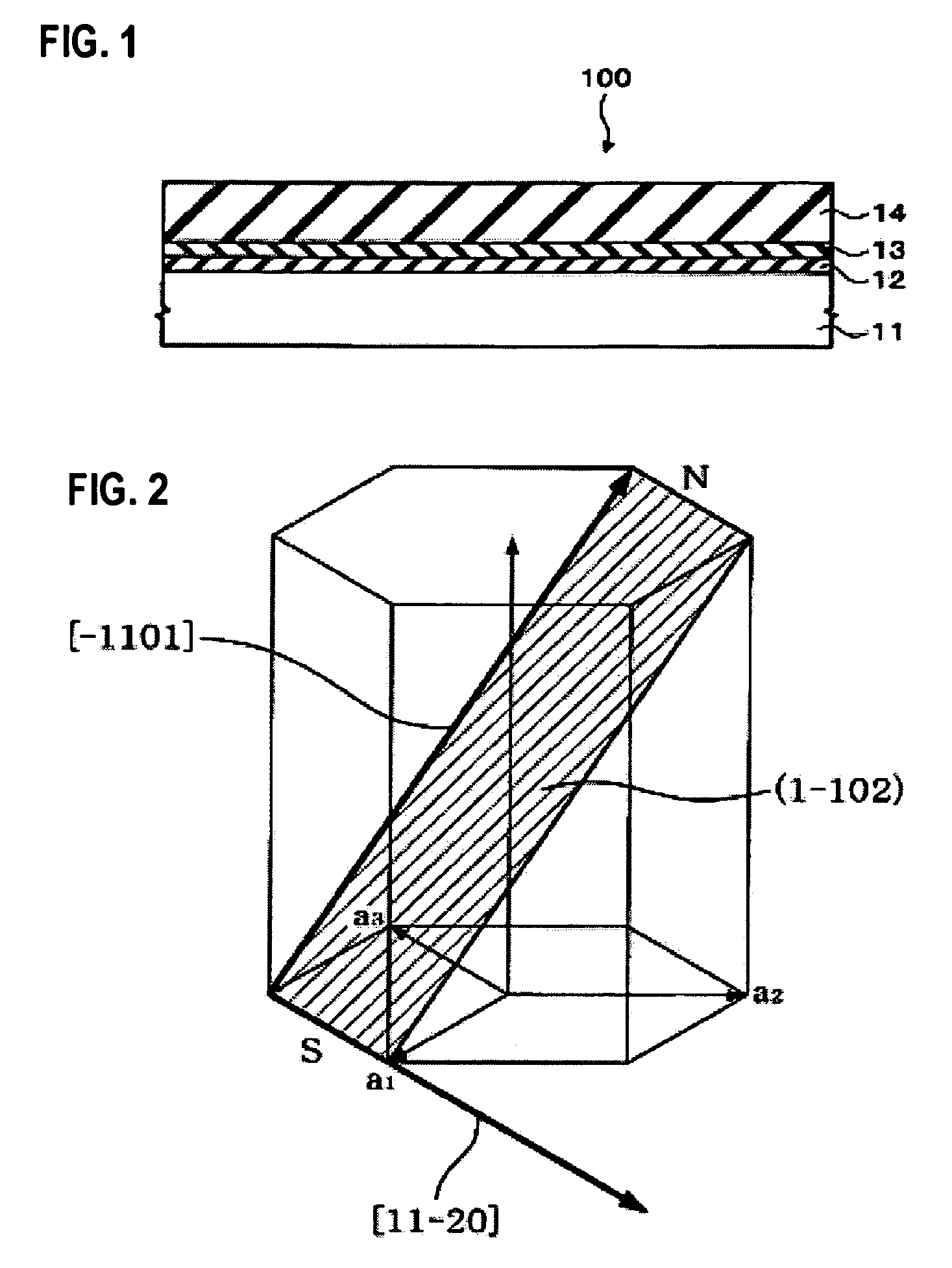
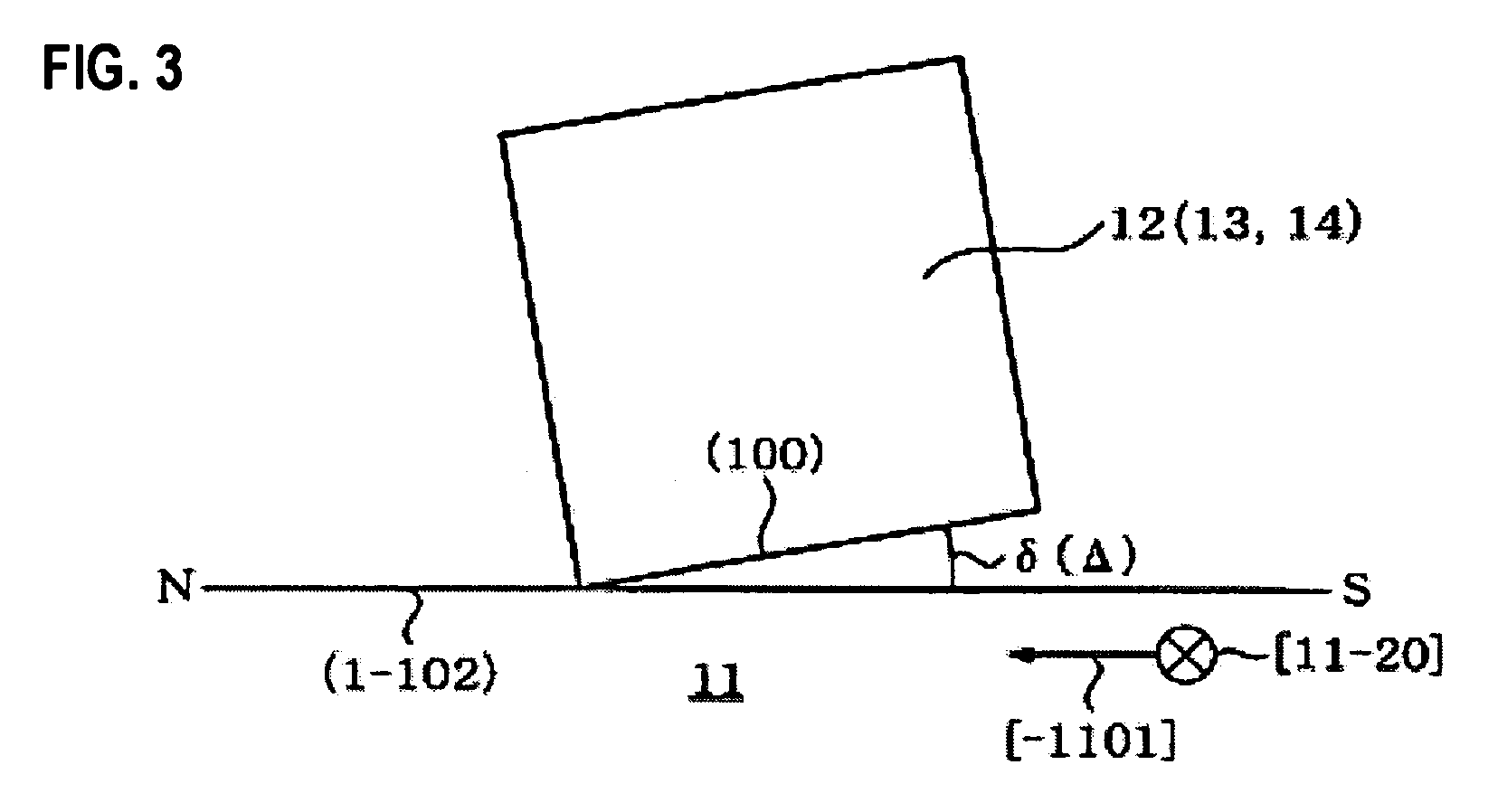
[0082]1.1. FIG. 1 is a cross-sectional view schematically showing a potassium niobate deposited body 100 in accordance with an embodiment of the invention. As shown in FIG. 1, the potassium niobate deposited body 100 of the present embodiment may include a substrate 11, a buffer layer 12 formed on the substrate 11, a lead zirconate titanate niobate layer 13 formed on the buffer layer 12, and a potassium niobate layer 14 formed on the lead zirconate titanate niobate layer 13.
[0083]An R-plane sapphire substrate may be used as the substrate 11. The use of an R-plane sapphire substrate is desirable because the buffer layer 12, the lead zirconate titanate niobate layer 13 and the potassium niobate layer 14 can be epitaxially grown thereon, a substrate with a large surface area can be obtained at a low price, and the R-plane sapphire substrate has a tolerance to etchant and can be used repeatedly.
[0084]As the buffer layer 12, for example, a metal oxide having a rock sal...
first experimental example
1.4. FIRST EXPERIMENTAL EXAMPLE
[0163]First, a substrate 11 composed of an R-plane sapphire single crystal plate was degreased and washed through soaking the substrate 11 in an organic solvent with an ultrasonic washing machine. As the organic solvent, a 1:1 mixed solution of ethyl alcohol and acetone was used. After loading the substrate 11 onto a substrate holder, the substrate 11 was introduced together with the substrate holder in a vacuum apparatus whose back pressure at room temperature was 1×10⁻⁷ Torr, oxygen gas was introduced such the oxygen partial pressure became 5×10⁻⁵ Torr, and then the substrate was heated to elevate its temperature to 400° C. at a rate of 20° C. / minute with an infrared ray lamp. At this time, as shown in FIG. 4A, a pattern obtained by the reflection high speed electron beam diffraction (i.e., reflection high energy electron diffraction: RHEED) in a sapphire [11-20] direction, diffraction patterns in streaks were observed.
[0164]Next, a pulsed beam of Kr...
second embodiment
2. Second Embodiment
[0183]2.1. FIG. 15 is a cross-sectional view schematically showing a potassium niobate deposited body 200 in accordance with an embodiment of the invention. The potassium niobate deposited body 200 of the present embodiment may include a substrate 11, a buffer layer 12 formed on the substrate 11, a first lead zirconate titanate niobate layer 13 formed on the buffer layer 12, a potassium niobate layer 14 formed on the first lead zirconate titanate niobate layer 13, and a second lead zirconate titanate niobate layer 15 formed on the potassium niobate layer 14. The present embodiment is different from the first embodiment in that the second lead zirconate titanate niobate layer 15 is further provided over the potassium niobate layer 14. Members that are similar to those of the potassium niobate deposited body 100 of the first embodiment are appended with the same reference numerals, and their detailed description shall be omitted.
[0184]An R-plane sapphire substrate ...
PUM
| Property | Measurement | Unit |
|---|---|---|
| angle | aaaaa | aaaaa |
| angle | aaaaa | aaaaa |
| crystallization temperature | aaaaa | aaaaa |
Abstract
Description
Claims
Application Information