Method for reducing the intrinsic stress of high density plasma films

a plasma film and intrinsic stress technology, applied in the direction of liquid surface applicators, chemical vapor deposition coatings, coatings, etc., can solve the problems of metal layers on device structures, substrate bowing or cracking, voids or other defects, narrow spaces or gaps, etc., to reduce the stress of films deposited, increase processing time, and reduce throughput

Inactive Publication Date: 2007-11-13
APPLIED MATERIALS INC
View PDF22 Cites 6 Cited by
  • Summary
  • Abstract
  • Description
  • Claims
  • Application Information

AI Technical Summary

Benefits of technology

[0012]The present invention provides a method and apparatus for reducing the stress of films deposited by HDP-CVD processes without substantially increasing processing time or decreasing throughput. The reduced stress layer is formed by delaying or interrupting application of a field that biases an HDP plasma toward a substrate.
[0014]In one embodiment of the apparatus of the present invention, a pedestal which holds a semiconductor substrate is located within a processing chamber. A gas distribution system introduces a process gas containing reactants into the vacuum chamber and sets and maintains a selected pressure in the chamber along with a vacuum pump and valve system. A plasma generation system creates an inductively coupled plasma from the process gas to form a first layer of the film being deposited. After deposition of the first layer, the plasma generation system further excites the plasma capacitively and biases the plasma toward the substrate. This enhances sputtering and forms the film's bulk layer. A processor controls the vacuum pump, gas distribution system and plasma generation system through a program stored in a connected memory.

Problems solved by technology

The high temperatures at which some thermal CVD processes operate can damage metal layers on device structures.
Intrinsic stress levels above or below certain values may cause a substrate to bow or crack or to form voids or other defects.
The result is narrow spaces or “gaps” (e.g., the space between metal lines) which are difficult to fill using conventional CVD methods.
Given these problems, the electrical and physical characteristics of some silicon oxide films deposited using some standard PECVD methods are no longer sufficient for many contemporary applications.
For a variety of reasons not yet well understood, however, films created in such HDP-CVD systems exhibit higher stress than those created in conventional capacitively coupled PECVD systems.
Controlling this increased stress is an important issue.
Such an approach, however, also increases processing time and thus decreases throughput as substrates are transferred from an HDP-CVD system to a PECVD or other type of system.
Even if deposition of the composite layer could take place in a single system, substrate throughput would still be adversely affected while process conditions such as pressure and temperature are adjusted for deposition of the two different layers.

Method used


Image

  • Method for reducing the intrinsic stress of high density plasma films
  • Method for reducing the intrinsic stress of high density plasma films
  • Method for reducing the intrinsic stress of high density plasma films

Examples


Embodiment Construction

I. An Exemplary High Density Plasma CVD System

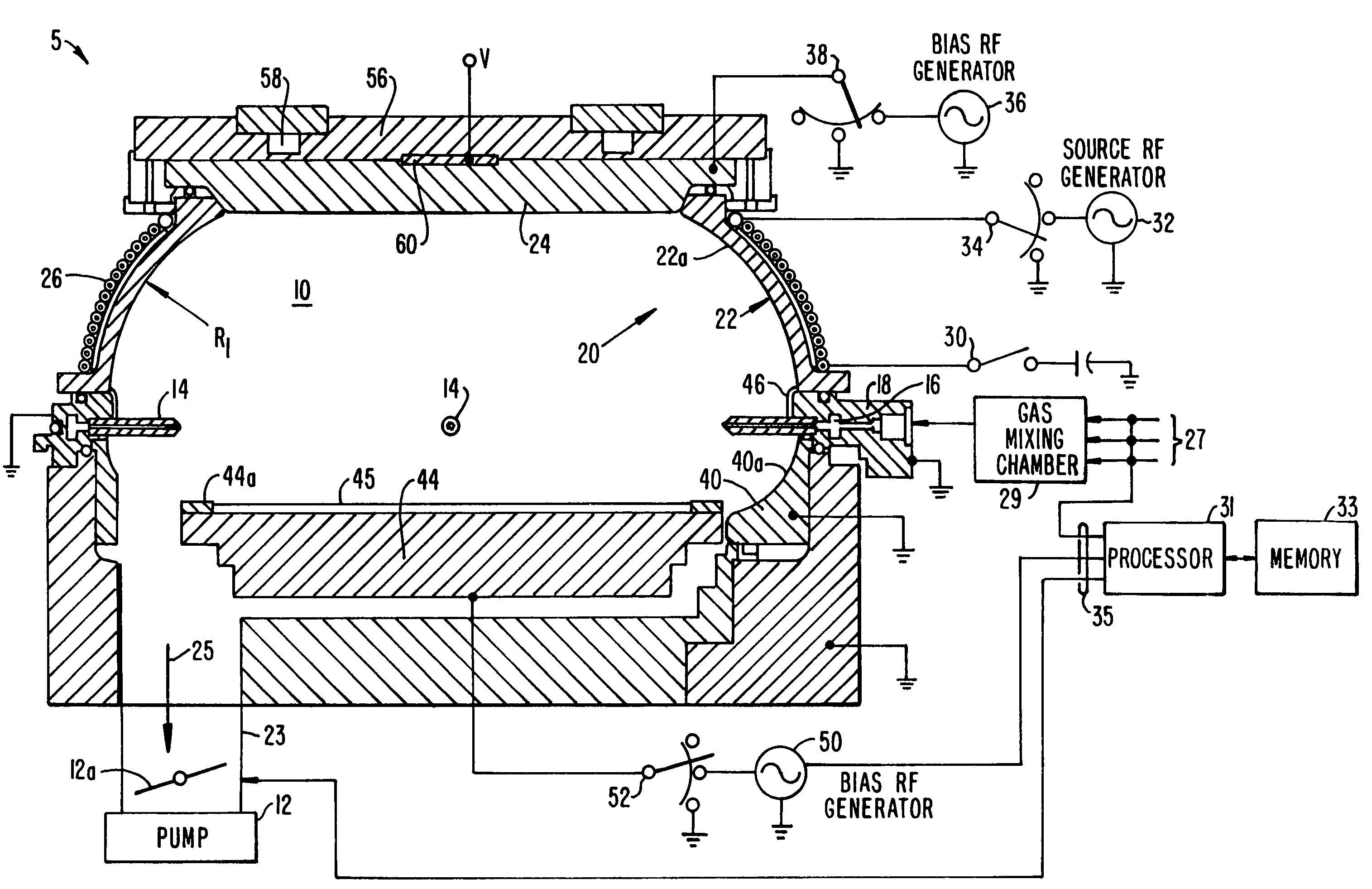
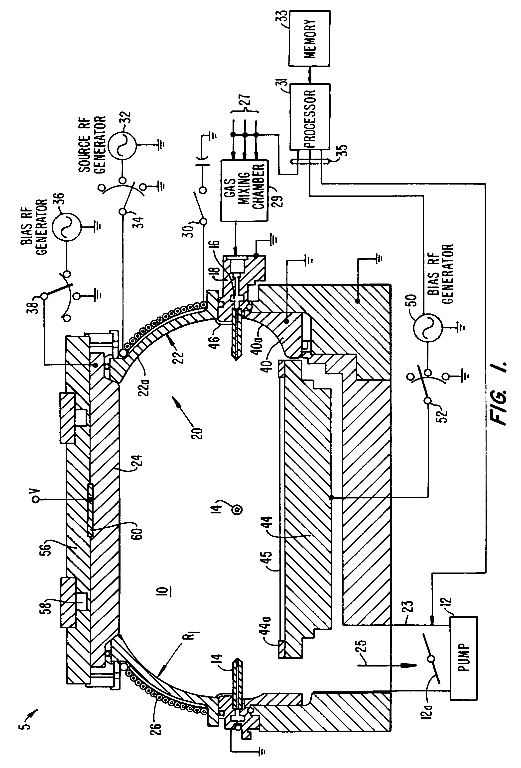
[0024]FIG. 1 illustrates one embodiment of an HDP-CVD system 5, capable of depositing a dielectric layer according to the present invention. HDP-CVD system 5 includes a vacuum chamber 10, a vacuum pump 12, a bias RF (BRF) generator 36, a BRF generator 50 and a source RF (SRF) generator 32.

[0025]Vacuum chamber 10 includes a ceiling 20 consisting of a sidewall 22 and a disk-shaped ceiling electrode 24. Sidewall 22 is made of an insulator such as quartz or ceramic and supports coiled antenna 26. The structural details of coiled antenna 26 are disclosed in U.S. patent application Ser. No. 08 / 113,776 entitled “High Density Plasma CVD and Etching Reactor,” by Fairbain and Nowak, filed Aug. 27, 1993, the disclosure of which is incorporated herein by reference.

[0026]Deposition gases and liquids are supplied through lines 27, having control valves (not shown), into a gas mixing chamber 29 where they are combined and sent to a gas supply ring mani...


PUM

PropertyMeasurementUnit
feature sizesaaaaaaaaaa
thicknessaaaaaaaaaa

Abstract

A layer of reduced stress is formed on a substrate using an HDP-CVD system by delaying or interrupting the application of capacitively coupled RF energy. The layer is formed by introducing a process gas into the HDP system chamber and forming a plasma from the process gas by the application of RF power to an inductive coil. After a selected period, a second layer of the film is deposited by maintaining the inductively-coupled plasma and biasing the plasma toward the substrate to enhance the sputtering effect of the plasma. In a preferred embodiment, the deposited film is a silicon oxide film, and biasing is performed by application of capacitively coupled RF power from RF generators to a ceiling plate electrode and wafer support electrode.

Description

[0001]This application is a divisional application of and claims the benefit of U.S. Application No. 08 / 623,445, filed Mar. 28, 1996 now U.S. Pat. No. 5,976,993, the disclosure of which is incorporated by reference.BACKGROUND OF THE INVENTION[0002]The present invention relates to the deposition of dielectric layers during semiconductor substrate processing. More specifically, the present invention relates to a method and apparatus for controlling the intrinsic stress in deposited layers. The method of the present invention is particularly useful in reducing the intrinsic stress of silicon oxide layers deposited by high density plasma chemical vapor deposition (HDP-CVD) techniques, but may be also applied to silicon oxide layers formed using other deposition methods, as well as to the deposition of silicon nitride and other layers.[0003]One of the primary steps in the fabrication of modern semiconductor devices is the formation of a thin film on a substrate by chemical reaction of ga...

Claims


Application Information

Patent Timeline
Patent Type & Authority Patents(United States)
IPC IPC(8): C23C16/50C23C16/503C23C16/515C23F1/00H01L21/306C23C16/24C23C16/40C23C16/517H01L21/316
CPCC23C16/402C23C16/517H01L21/02164H01L21/31612H01L21/02274H01L21/02304H01L21/02211H01L21/306
Inventor RAVI, K. V.ROSSMAN, KENTSAHIN, TURGUTNARWANKAR, PRAVIN
Owner APPLIED MATERIALS INC
Why Eureka
Try Eureka