Method of and apparatus for measuring stress of semiconductor material

a technology of stress measurement and semiconductor material, which is applied in the direction of optical radiation measurement, instruments, spectrometry/spectrophotometry/monochromators, etc., can solve the problems of large error in a predetermined stress measurement, inability to measure the raman spectrum of the sige layer b>3/b>c, and become very difficult to ensure predetermined measurement accuracy and measurement reproducibility, etc., to achieve high degree of accuracy, high speed, and accura

Inactive Publication Date: 2007-11-13
HORIBA LTD
View PDF8 Cites 19 Cited by
  • Summary
  • Abstract
  • Description
  • Claims
  • Application Information

AI Technical Summary

Benefits of technology

[0022]A current temperature of the measured semiconductor material is estimated from the peak position shift amount of the Raman spectrum in the non-stress state from the substrate obtained by irradiating the excitation light so as to reach the single crystal silicon substrate, and the peak position shift amounts of the Raman spectrum in the strained silicon layer and in the silicon germanium layer (SiGe layer) stacked on one another on the substrate are corrected so that the stresses of the strained silicon layer and the SiGe layer can be accurately measured irrespective of, for example, any variations in the optical system such as a wavelength shift due to any strained optical component and a deteriorated optical filter resulting from changing ambient temperature, which causes the peak position shift of the Raman spectrum, influenced by the temperature of the measured semiconductor material itself, and the like. Therefore, it becomes unnecessary to provide a temperature adjusting mechanism for maintaining the temperature of the semiconductor material itself at a constant degree and the additional steps such as measuring the Raman spectrum of the specimen for correcting the temperature, which is prepared apart from the semiconductor material, prior to the measurement of the semiconductor material as the measuring object so as to correct the peak position of the Raman spectrum influenced by the temperature change of the semiconductor material based on the measurement information. As a result, stress can be measured with a high degree of accuracy, at a high speed and at a low cost free from any influence from temperature. Further, such a highly accurate and high-speed stress measurement can be reproduced in a stable manner for a long period of time. Thereby, as a result of such an effect, the productivity of a semiconductor device provided with the semiconductor material using the strained silicon can be greatly improved.
[0023]Further, as described, not only the predetermined stress calculation but also the calculation of the respective physical quantities such as the film thicknesses of the strained silicon layer and SiGe layer and / or the Ge content in the SiGe layer and the like can be implemented using the shift amount of the peak position, spectral full width at half maximum, spectral intensity, spectral area and the like in each of the layers constituting the semiconductor material as parameters. Thereby, quality control in the semiconductor material can achieve a higher performance so that the quality of the manufactured semiconductor device can be further improved, and the inspecting steps and facility can be simplified possibly leading to productivity improvement and the reduction of the manufacturing cost.
[0024]Further, a plurality of laser sources having different wavelengths are provided in the Raman spectroscopic system, and any of the laser beams having the different wavelengths from the laser sources can be selectively irradiated on the semiconductor material. Accordingly, the excitation light can unfailingly reach the substrate irrespective of what general thickness and thickness ratios of the respective layers the measured semiconductor material has. Then, the temperature of the semiconductor material can be accurately estimated based on the peak position shift amount of the Raman spectrum from the substrate and the peak position shift amounts of the Raman spectra in the strained silicon layer and the SiGe layer can be accurately corrected based on the estimated temperature. As a result, a predetermined stress measurement achieving a high accuracy and a high speed can be reliably and stably implemented.

Problems solved by technology

Therefore, when the generally available Raman spectroscopic technology is directly applied to the measurement of the stress of the strained silicon, it becomes very difficult to assure a predetermined measurement accuracy and measurement reproducibility.
On the other hand, when the laser having a small wavelength and a small penetration depth is used, the excitation light does not reach the SiGe layer 3C, which makes it impossible to measure the Raman spectrum of the SiGe layer 3C.
While it is possible to avoid any influence from the changing ambient temperature by controlling the variations of the optical system caused by the change of the ambient temperature by means of the conventional method recited in No. 2001-66197 of the Publication of the Unexamined Japanese Patent Application in the case of measuring the Raman spectrum of the strained silicon layer 3D using the ultraviolet light as the excitation light, the influence received from the temperature change of the measured semiconductor material itself easily results in the generation of a large error in a predetermined stress measurement.
Therefore, in the pursuit of assuring a highly accurate measurement undergoing fewer errors and stable measurement reproducibility in a long period of time, a temperature adjusting mechanism for maintaining the temperature of the semiconductor material at a constant degree or the like and a number of additional steps are unfavorably required in order to avoid any influence from the temperature change of the measured material itself.
As a result, a remarkable deterioration of a productivity is triggered by incorporating the measurement of the stress of the semiconductor material having the foregoing disadvantages into the manufacturing line in which a high speed and continuity are demanded, such as the manufacturing of the semiconductor device.
Thus, it is practically not possible to introduce such a stress measurement.
As described, the conventional method included such problems that the measurement accuracy was inevitably lowered due to the shift of the peak position of the Raman spectrum in accordance with the temperature change of the measured material itself and the measurement reproducibility could not be assured in a long term.

Method used


Image

  • Method of and apparatus for measuring stress of semiconductor material
  • Method of and apparatus for measuring stress of semiconductor material
  • Method of and apparatus for measuring stress of semiconductor material

Examples


first embodiment

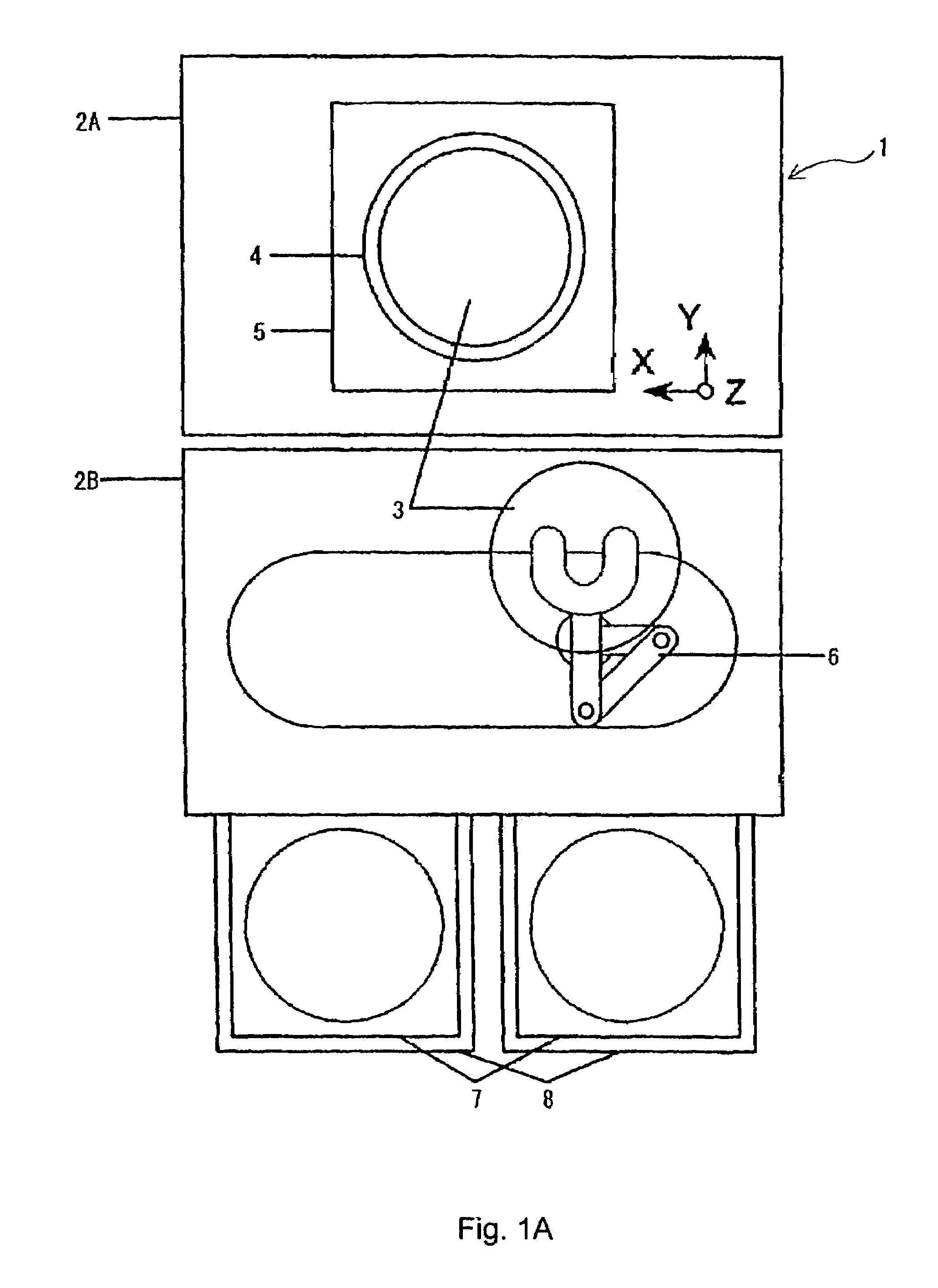
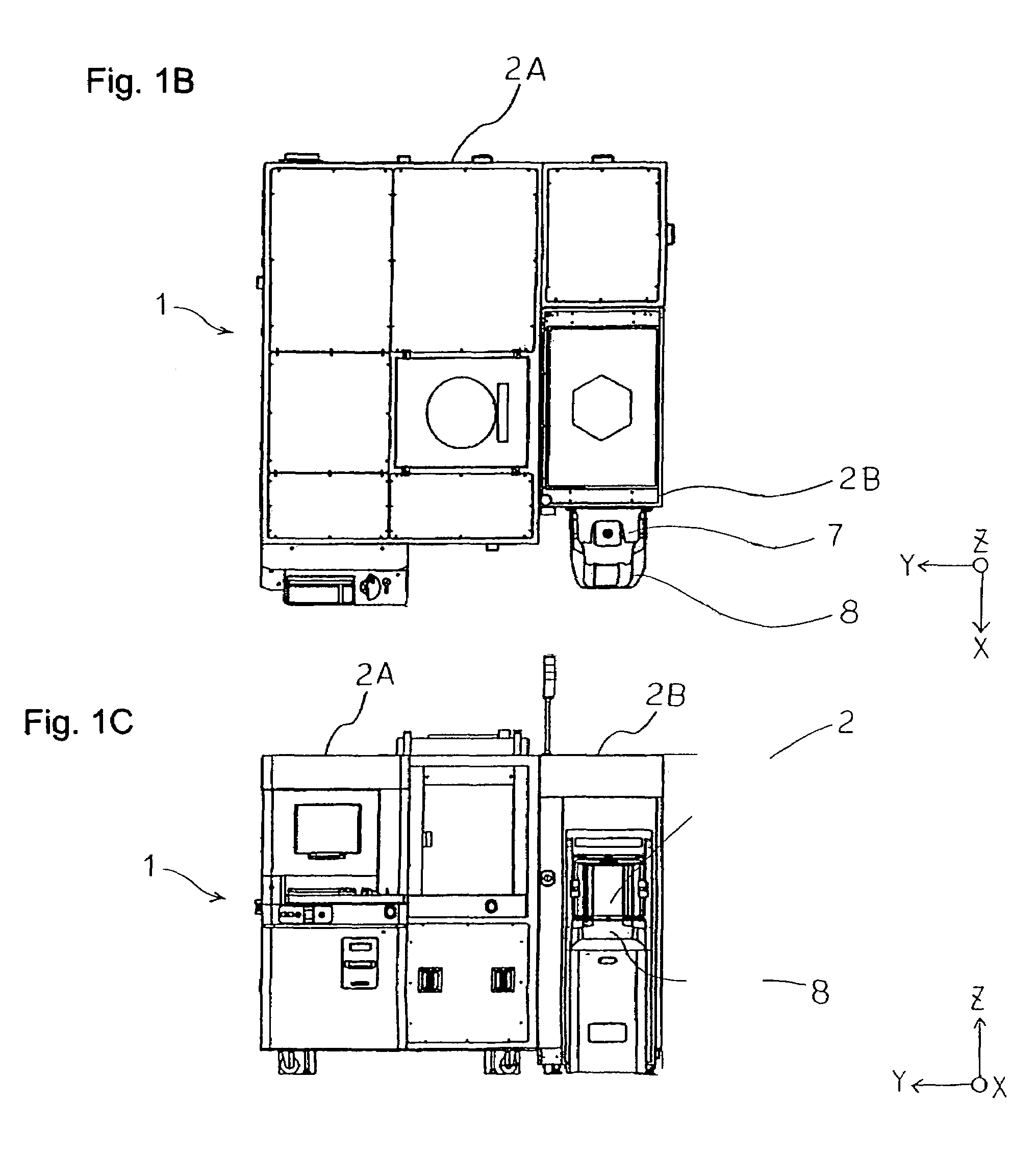
[0042]FIG. 1A is a plan view schematically showing an entire configuration of a substrate inspection apparatus 1 according to the present invention and FIG. 2 is a view showing a configuration of a stress measuring system as a main part of the substrate inspection apparatus 1. In FIG. 1A, 2A is a measuring chamber of the substrate inspection apparatus 1 equipped with a Raman spectroscopic optical system / ellipsometric optical system, 2B is a transport equipment set up next to the measuring chamber 2A, 3 is a substrate (sample, hereinafter referred to as a wafer) of for example, a silicon wafer formed by applying the strained silicon technique where the thin film of silicon layer is formed on the SiGe layer with large lattice constant, 4 is a sample stage configured so as to be movable in a three-dimensional direction of horizontal direction (X, Y directions) and height direction (Z direction), and 5 is a driving section of the sample stage 4.

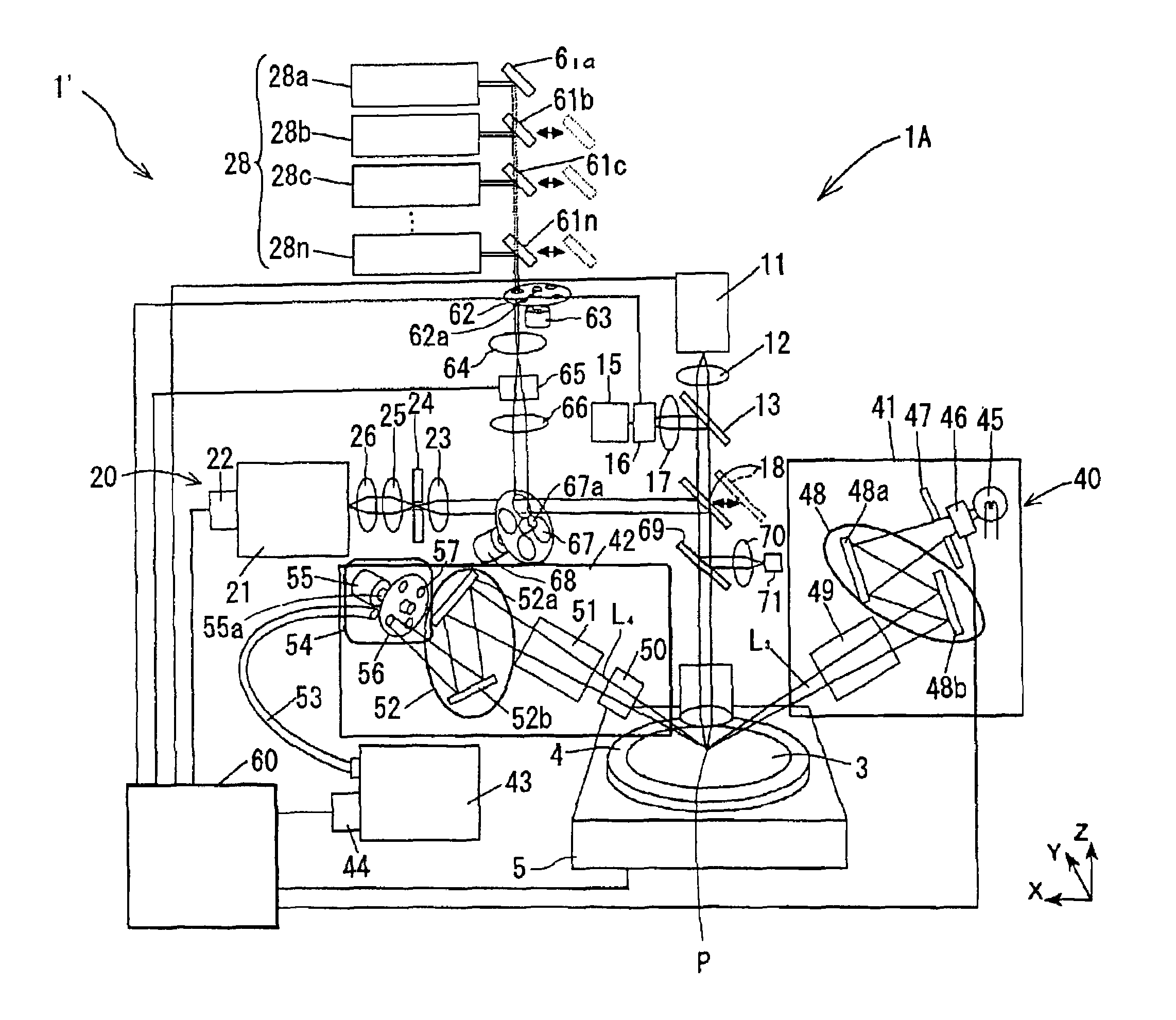
[0043]In FIG. 1A, 6 is a robot arm with a ...

second embodiment

[0107]In the substrate inspection apparatus 1′ not only the stresses σ1 and σ2 of the strained silicon layer 3D and the SiGe layer 3C can be measured by the Raman spectroscopic optical system 20, but also the film thickness and the refractivity can be highly accurately measured by the ellipsometer optical system 40. Thereby, when the semiconductor substrate using the strained silicon, which has been increasingly used in the manufacturing of the semiconductor device in recent years, is used as the measuring object, the respective physical quantities such as the internal stresses of the strained silicon layer 3D and the SiGe layer 3C which is the ground layer thereof and the Ge content in the SiGe layer 3C can be reliably measured so that the substrate can be highly accurately inspected.

[0108]However, because the present invention is aimed at measuring the stresses of the strained silicon layer 3D and the SiGe layer 3C which is the ground layer thereof in the semiconductor material (...


PUM

PropertyMeasurementUnit
wavelengthsaaaaaaaaaa
temperatureaaaaaaaaaa
wavelengthaaaaaaaaaa

Abstract

The present invention provides a method of and a device for measuring the stress in a semiconductor material. An excitation light is irradiated on a semiconductor material formed with a silicon germanium layer and a strained silicon layer in a multilayer structure on a single crystal silicon substrate from the direction of the strained silicon layer. An internal stress of the semiconductor material is measured from peak position information of the Raman spectrum of scattered light from the irradiating point, wherein light having a wavelength capable of reaching the single crystal silicon substrate is used as the excitation light, a temperature of the semiconductor material is estimated from a shift amount of the peak position of the Raman spectrum of the scattered light from the substrate in accordance with the irradiation of the excitation light and the shift amounts of the peak positions of the Raman spectra in the strained silicon layer and in the silicon germanium layer are corrected by means of the estimated temperature, The internal stresses of the strained silicon layer and the silicon germanium layer are calculated from the corrected peak position information of the Raman spectra in the respective layers.

Description

BACKGROUND OF THE INVENTION[0001]1. Field of the Invention[0002]The present invention relates to a method of and a apparatus for measuring stress in a semiconductor material and for automatically measuring internal stresses of a thin film formed on a surface of a semiconductor substrate such as a silicon wafer or the like and fine processing parts variously patternized, which is incorporated into a manufacturing line of a semiconductor device or the like as a method of inspecting a product and a product material.[0003]2. Description of Related Art[0004]In a semiconductor device manufacturing process, quality control through the measurement of stresses of a thin film formed on a surface of a semiconductor substrate such as a silicon wafer or the like and fine processing parts of different patterns, a film thickness, a composition and the like is an significantly important and indispensable element for maintaining a stable performance of the manufactured semiconductor device.[0005]In ...

Claims


Application Information

Patent Timeline
Patent Type & Authority Patents(United States)
IPC IPC(8): G01J3/44G01N21/21G01N21/65G01N21/84G01N21/95
CPCG01N21/211G01N21/9501G01N21/65G01J3/44G01N2021/8477
Inventor NAKA, NOBUYUKIKATANISHI, AKIHIROMAGARI, MASAAKI
Owner HORIBA LTD
Why Eureka
Try Eureka