Nanoscale wires and related devices

a technology of nano-scale wires and related devices, applied in the field of nano-scale semiconductors, can solve the problems that the field of nano-scale electronics is not well-developed

Inactive Publication Date: 2007-11-27
PRESIDENT & FELLOWS OF HARVARD COLLEGE
View PDF210 Cites 150 Cited by
  • Summary
  • Abstract
  • Description
  • Claims
  • Application Information

AI Technical Summary

Problems solved by technology

While nanoscopic articles might be well-suited for transport of charge carriers and excitons (e.g. electrons, electron pairs, etc.) and thus may be useful as building blocks in nanoscale electronics applications, other than standard small-scale lithographic techniques, nanoelectronics is not a well-developed field.

Method used


Image

  • Nanoscale wires and related devices
  • Nanoscale wires and related devices
  • Nanoscale wires and related devices

Examples


example 1

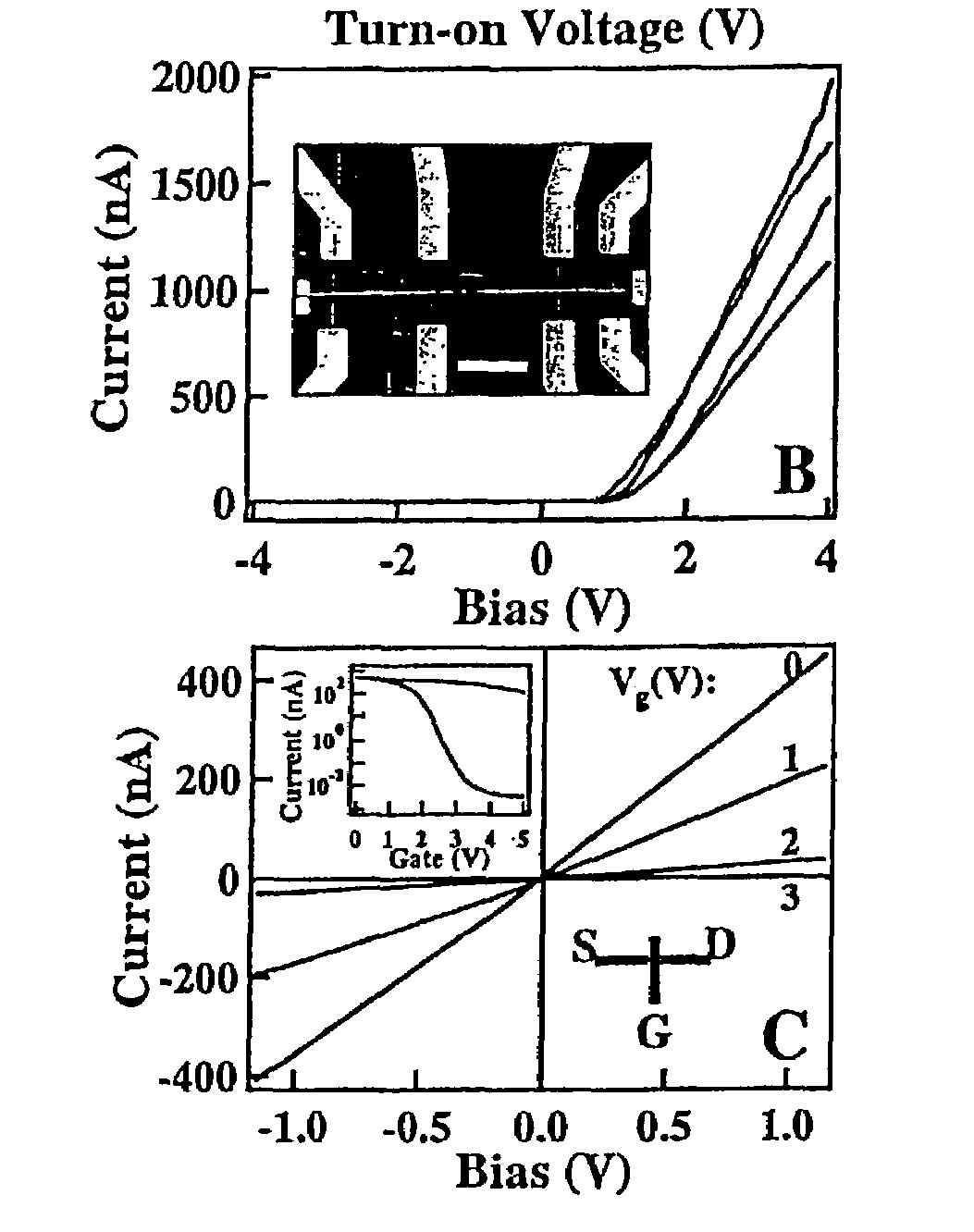
[0315]Single crystal n-type and p-type silicon nanowires (SiNWs) were prepared and characterized by electrical transport measurements. As used herein, a “single crystal” item is an item that has covalent bonding, ionic bonding, or a combination thereof throughout the item. Such a single crystal item may include defects in the crystal, but is distinguished from an item that includes one or more crystals, not ionically or covalently bonded, but merely in close proximity to one another. Laser catalytic growth was used to introduce controllably either boron or phosphorous dopants during the vapor phase growth of SiNWs. Estimates of the carrier mobility made from gate-dependent transport measurements are consistent with diffusive transport. In addition, these studies show it is possible to heavily dope SiNWs and approach a metallic regime. Temperature-dependent measurements made on heavily doped SiNWs show no evidence for coulomb blockade at temperature down to 4.2 K, and thus testify to...

example 2

[0331]Nearly monodisperse samples of single crystalline GaP nanowires were synthesized with diameters of 10, 20, and 30 nm and lengths greater than 10 μm by exploiting well-defined gold colloids as catalysts in this laser catalytic growth (LCG) process. In this method, the Ga and P reactants generated by laser ablation of solid GaP are subsequently directed into a nanowire structure by gold nanocluster catalysts. Transmission electron microscopy (TEM) studies of nanowires prepared in this way demonstrate that the distributions of nanowire diameters are defined by those of the nanocluster catalysts. High-resolution TEM shows that the wires are single crystal zinc blend with a [111] growth direction, and energy dispersive X-ray analysis confirms that the nanowire composition is stoichiometric GaP. The use of monodisperse nanocluster catalysts combined with the LCG method enablesthe growth of a wide range of semiconductor nanoscale wires with well-defined and controlled diameters, and ...

example 3

[0340]The synthesis of a broad range of multicomponent semiconductor nanoscale was accomplished using laser-assisted catalytic growth. Nanoscale wires of binary group III-V materials (GaAs, GaP, InAs and InP), ternary III-V materials (GaAs / P, InAs / P), binary II-VI compounds (ZnS, ZnSe, CdS, and CdSe) and binary SiGe alloys were prepared in bulk quantities as high purity (>90%) single crystals. The nanoscale wires have diameters varying from three to tens of nanometers, and lengths extending to tens of micrometers. The synthesis of this wide range of technologically important semiconductor nanoscale wires can be extended to many other materials.

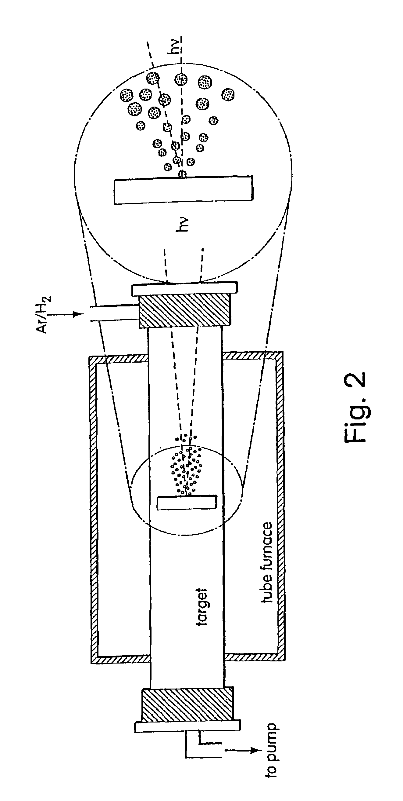
[0341]The present technique involves the growth of elemental Si and Ge nanoscale wires using the LCG method, which uses laser ablation to generate nanometer diameter catalytic clusters that define the size and direct the growth of the crystalline nanoscale wires by a vapor-liquid-solid (VLS) mechanism. A key feature of the VLS growth process a...


PUM

PropertyMeasurementUnit
widthaaaaaaaaaa
widthaaaaaaaaaa
widthaaaaaaaaaa

Abstract

The present invention relates generally to sub-microelectronic circuitry, and more particularly to nanometer-scale articles, including nanoscale wires which can be selectively doped at various locations and at various levels. In some cases, the articles may be single crystals. The nanoscale wires can be doped, for example, differentially along their length, or radially, and either in terms of identity of dopant, concentration of dopant, or both. This may be used to provide both n-type and p-type conductivity in a single item, or in different items in close proximity to each other, such as in a crossbar array. The fabrication and growth of such articles is described, and the arrangement of such articles to fabricate electronic, optoelectronic, or spintronic devices and components. For example, semiconductor materials can be doped to form n-type and p-type semiconductor regions for making a variety of devices such as field effect transistors, bipolar transistors, complementary inverters, tunnel diodes, light emitting diodes, sensors, and the like.

Description

[0001]This application is a continuation-in-part of U.S. Ser. No. 10 / 152,490, filed May 20, 2002 now abandoned, which claims priority to U.S. Ser. No. 60 / 292,045, filed May 18, 2001, and to U.S. Ser. No. 60 / 291,896, filed May 18, 2001, and to U.S. Ser. No. 60 / 354,642, filed Feb. 6, 2002, and to U.S. Ser. No. 60 / 348,313, filed Nov. 9, 2001; which U.S. Ser. No. 10 / 152,490 also is a continuation-in-part of U.S. Ser. No. 09 / 935,776, filed Aug. 22, 2001 now abandoned, which claims priority to U.S. Ser. No. 60 / 226,835, filed Aug. 22, 2000, and to U.S.S.N. 60 / 292,121, filed May 18, 2001; and which U.S. Ser. No. 10 / 152,490 also is a continuation-in-part of U.S. Ser. No. 10 / 020,004, filed Dec. 11, 2001 now U.S. Pat. No. 7,129,554, which claims priority to U.S. Ser. No. 60 / 292,035, filed May 18, 2001 and to U.S. Ser. No. 60 / 254,745, filed Dec. 11, 2000.PRIORITY APPLICATIONS[0002]This application claims the benefit of priority under 35 U.S.C. §120 of U.S. patent application Ser. No. 10 / 152,490...

Claims


Application Information

Patent Timeline
Patent Type & Authority Patents(United States)
IPC IPC(8): H01L29/76H01L29/06H01L29/94C30B11/00C30B25/00G01N27/12G01N27/414G01N33/543G01Q70/00G11C11/56G11C13/02H01L23/532H01L29/20H01L29/207H01L29/267H01L29/73H01L31/0352H01L31/08H01L33/18H01L51/00H01L51/30
CPCB82Y10/00C30B11/00C30B25/00C30B25/005C30B29/60G01N33/54373G11C11/56G11C13/0014G11C13/0019G11C13/025H01L21/02532H01L21/0254H01L21/02543H01L21/02546H01L21/02557H01L21/0256H01L21/02603H01L21/02628H01L21/02645H01L21/02653H01L23/53276H01L29/0665H01L29/0673H01L29/0676H01L29/068H01L29/125H01L29/1606H01L29/2003H01L29/207H01L29/267H01L29/73H01L29/7781H01L29/78696H01L29/861H01L29/868H01L31/0352H01L31/08H01L51/0048G01N27/4146C30B29/605B82Y15/00B82Y30/00G11C13/04G11C2213/17G11C2213/18G11C2213/77G11C2213/81H01L21/02617H01L27/092H01L33/18H01L51/0595H01L2924/12044H01L2924/3011Y10S977/936Y10S977/958Y10S977/938Y02E10/549H01L2924/0002Y10T428/298Y10T428/2929H01L2924/00A61B5/1468A61B5/14542A61B5/14532A61B2562/0285A61B5/1455A61B5/14539A61B5/685A61B5/1473H10K85/221H10K10/701
Inventor LIEBER, CHARLES M.DUAN, XIANGFENGCUI, YIHUANG, YUGUDIKSEN, MARKLAUHON, LINCOLN J.WANG, JIANFANGPARK, HONGKUNWEI, QINGQIAOLIANG, WENJIESMITH, DAVID C.WANG, DELIZHONG, ZHAOHUI
Owner PRESIDENT & FELLOWS OF HARVARD COLLEGE
Why Eureka
Try Eureka