Eureka AIR delivers breakthrough ideas for toughest innovation challenges, trusted by R&D personnel around the world.

Actively stabilized, single input beam, interference lithography system and method

a lithography system and interference technology, applied in the field of interference lithography techniques, can solve the problems of limited practical limitations, insufficiently realized advantages in high-volume manufacturing environments, and use of division-of-wavefront il in applications requiring the fabrication of structures which vary in two dimensions, and achieve active stabilization and enhanced wavefront-division interference lithography configuration.

Inactive Publication Date: 2007-12-04
AZTEC SYST
View PDF4 Cites 10 Cited by
  • Summary
  • Abstract
  • Description
  • Claims
  • Application Information

AI Technical Summary

Benefits of technology

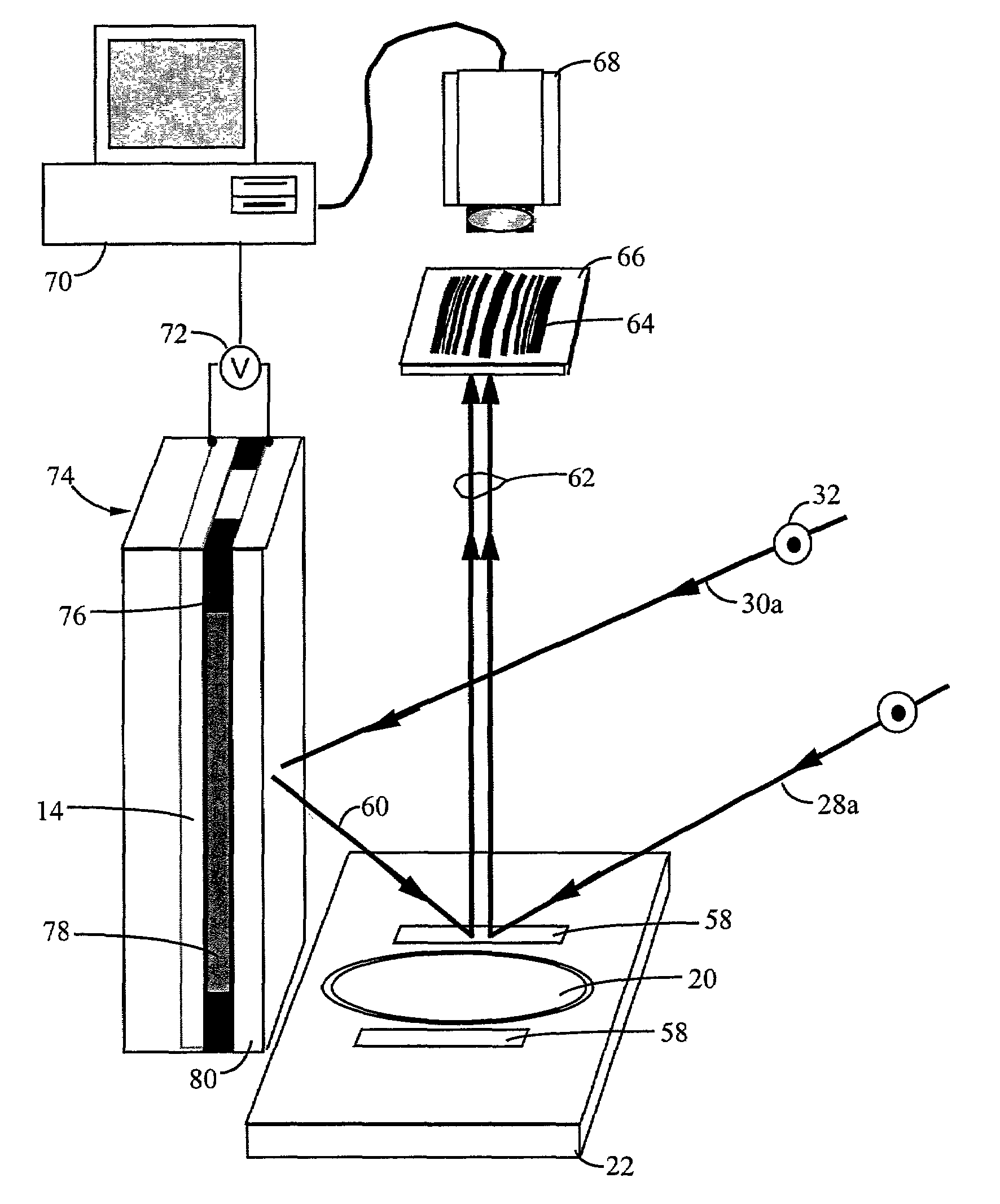
[0019]With this background in mind, the inventive device described herein provides an actively stabilized, interference lithography system suitable for exposing light sensitive materials in production environments. Specifically, the wavefront-division interference lithography configuration is enhanced through the incorporation of a novel feedback mechanism and an unconventional phase modulation device allowing the system to be actively stabilized.
[0020]The inventive device allows for the high-volume, low cost production of surface structures for novel biomedical devices and sensors, grating structure alignment layers and tunable wavelength resonance gratings for reflective LCDs, flat panel array structures for FED displays, and motheye surface relief antireflection patterns.
[0026]The objects of the present invention may be attained generally by providing a manufacturing device optionally consisting of seven major components: one, a source of polarized, coherent optical radiation with a wavelength suitable for exposing light sensitive materials such as that derived from a laser; two, a flexible, re-configurable beam delivery system with a means to expand or enlarge a single beam and propagate said beam over a distance sufficient to achieve minimal variation in pattern pitch; three, a means for apodizing the source beam to produce a more efficient energy distribution at the recording plane containing the light sensitive material; four, a division of wavefront system consisting of at least one mirror or prism where the diameter of the input beam is divided into two, three, or more sections, with each section redirected so as to overlap in a common region of space; five, a means for dynamically sensing and compensating for relative phase drifts between the divided beam sections; six, a means for enhancing the passive stability of the system to dampen typical manufacturing environment acoustical and mechanical vibrations; and seven, a mechanized stage with translation and rotation providing a wafer mount, and computer controller for replicating the patterning area over arbitrarily large substrates.

Problems solved by technology

These advantages have not been fully realized in high-volume manufacturing environments since existing methods for actively stabilizing the interference patterns produced by a division-of-wavefront configuration, have not been practical.
In addition, the use of division-of-wavefront IL in applications requiring the fabrication of structures which vary in two dimensions, has been limited due to the lack of a practical method for optimizing the interference pattern contrast, and the additional complexity of incorporating an active stabilization system which operates on more than one divided beam section.
The first two techniques suffer from practical limitations such as small field size, stitching errors, short mask lifetimes, low throughput, and high cost.
However, as the size of the grating features is reduced toward the 100 nanometer sizes needed for DFB lasers operating about the 1300 nm wavelength, small mechanical and thermal disturbances in the system become significant, and consequently manufacturers find that their yields are low and that their systems require highly skilled operators.
This technique is not readily implemented in the folding mirror division-of-wavefront IL system due to the close proximity of the interfering beams.
However, traditionally a moving mirror has been considered impractical for the division of-wavefront IL system because of the large size of the mirror required.
This system was limited due to the precise alignment needed to produce an observable macroscopic fringe pattern, and the need to fabricate a new grating for each pattern pitch desired.
These patterns are limited by the resolution and field size of the imaging or writing systems, and complex, often expensive, workaround solutions are required to achieve modest field sizes of 50×50 mm with hole diameters in the 1 to 2 micron range.
A means for manufacturing motheye structures in high volumes and over large-areas is not currently available.

Method used


Image

  • Actively stabilized, single input beam, interference lithography system and method
  • Actively stabilized, single input beam, interference lithography system and method
  • Actively stabilized, single input beam, interference lithography system and method

Examples


Embodiment Construction

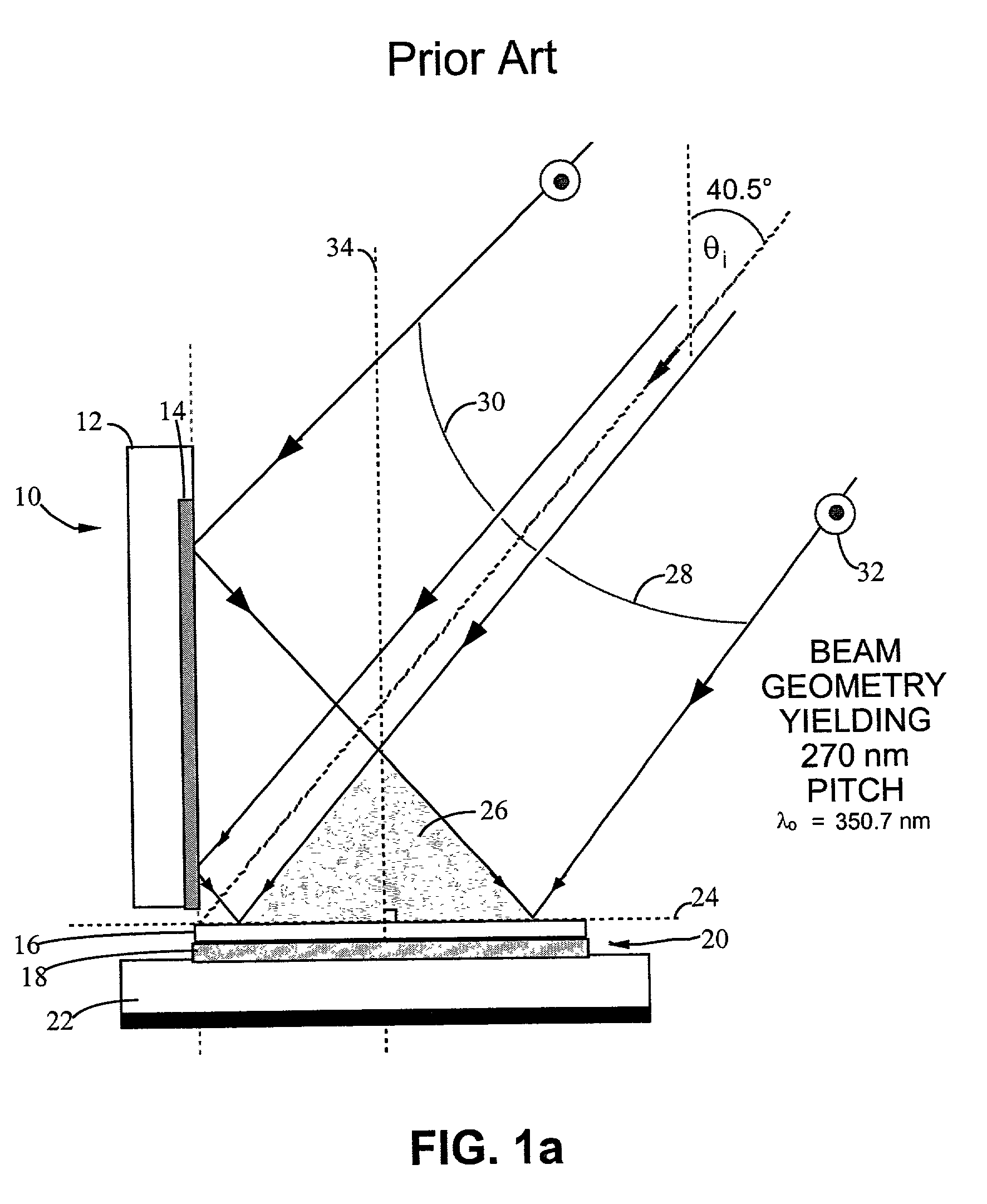
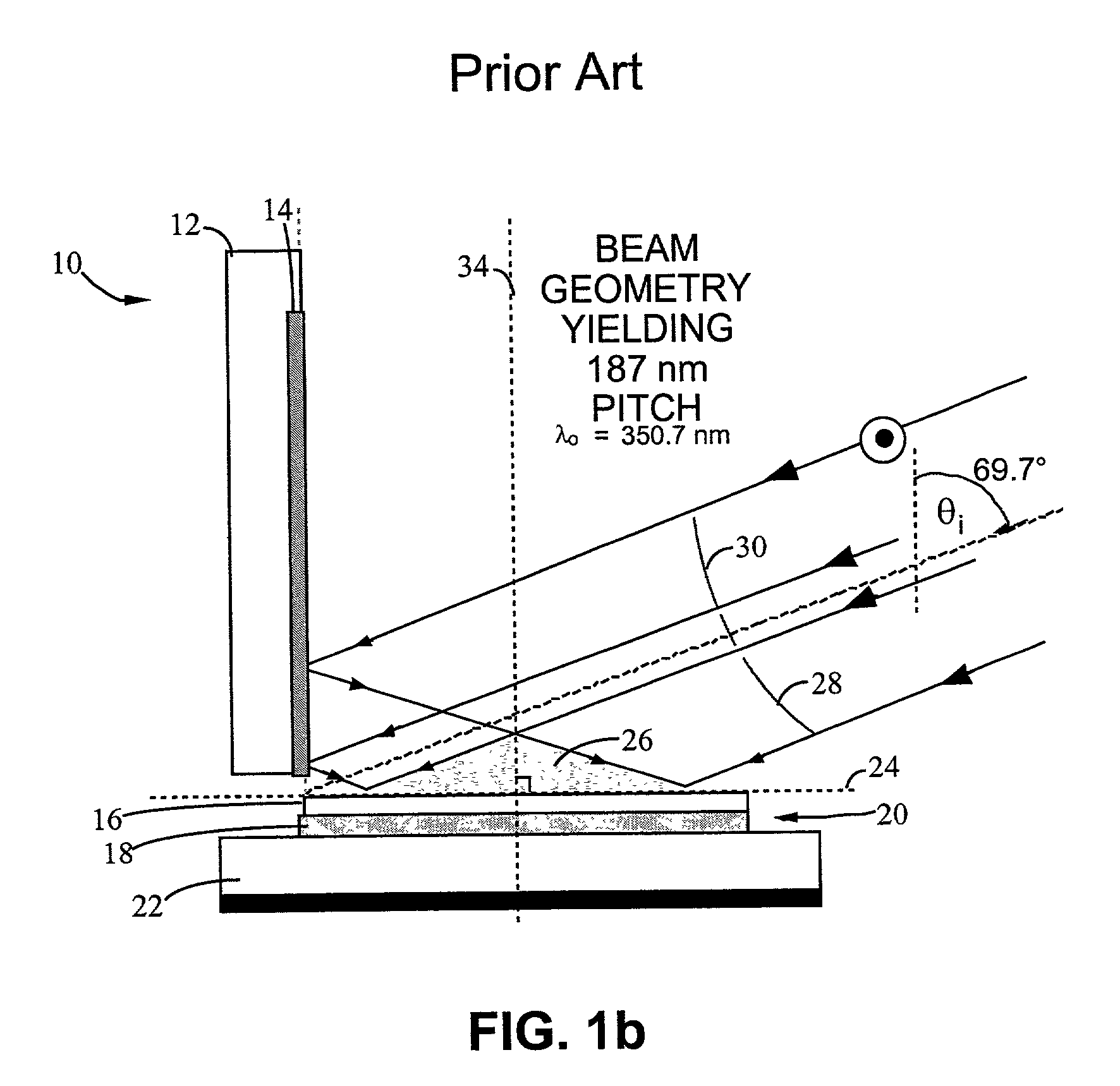
[0055]As used herein, a workpiece is defined to include a layer of light sensitive material by itself or in combination with other layers of materials, such as a substrate and / or other intervening layers, including planar, non-planar and irregularly shaped objects. For example, the workpiece can be a wafer or a panel. In the exemplary embodiment shown in FIGS. 1a and 1b, workpiece 20 is a wafer comprised of an indium phosphide substrate 18 with a photoresist coating 16 having a thickness in the range of from 1000 to 2000 angstroms(Å). As used herein, the term platform includes any mounting mechanism to which the workpiece can be secured in a desired position and orientation, including but not limited to a wafer stage and vacuum chuck arrangement. Optionally, the position of the platform can be controlled to correctly position the workpiece relative to the interference pattern produced by the optical configuration (e.g., the platform can be rotated and translated to insert and remove...


PUM


Abstract

An interference lithography system is described that is capable of exposing high resolution patterns in photosensitive media and employing yield increasing active stabilization techniques needed in production environments. The inventive device utilizes a division-of-wavefront interference lithography configuration which divides a single large field size optical beam using one or more mirrors, and is actively stabilized with a subsystem employing; a phase modulator operating on each divided wavefront section; a novel feedback apparatus for observing the relative phase shifts between interfering wavefront sections; and a control system for holding the relative phase shifts constant. The present invention also includes; a method for shaping the illumination beam's intensity distribution for more efficient power utilization and greater feature size uniformity; a horizontal substrate loading configuration compatible with robotic handling; an automated pattern pitch calibration for simple, flexible system reconfiguration; a compact clean-room compatible superstructure for increased passive stability in high vibration manufacturing environments; and a method for optimizing the polarization state of the interfering beam sections in a multiple mirror system.

Description

CROSS REFERENCE TO THE RELATED APPLICATION[0001]This application claims priority from U.S. Provisional Patent Application Ser. No. 60 / 186,893, entitled “Actively Stabilized, Single Input Beam, Interference Lithography Tool For Production Environments,” filed Mar. 3, 2000. The disclosure of this provisional patent application is incorporated herein by reference in its entirety.BACKGROUND OF THE INVENTION[0002]1. Field of the Invention[0003]The present invention relates to interference lithography techniques capable of generating periodic arrays of sub-micron sized structures. Specifically, wavefront division (WD) interference lithography is enhanced through the incorporation of a novel active stabilization technique. In addition, the disclosed invention relates to the incorporation of actively stabilized WD interference lithography in a flexible configuration, high-throughput, production-worthy system. Such a system finds countless applications in the telecommunications, display, bio...

Claims


Application Information

Patent Timeline
IPC IPC(8): G03H1/12G03H1/04G03H1/10G03F7/20G03H1/00
CPCG03F7/70408G03H1/00G03H2001/0094
Inventor HOBBS, DOUGLAS S.COWAN, JAMES J.
Owner AZTEC SYST
Why Eureka
Eureka Blog
Learn More