Methods to minimize contact resistance

a technology of contact resistance and minimizing cost, which is applied in the direction of solid-state devices, organic semiconductor devices, material nanotechnology, etc., can solve the problems of low efficiency of tft circuits, and high cost of silicon-based tft circuits. achieve the effect of increasing the conductivity of semiconductors and reducing contact resistan

Active Publication Date: 2007-12-11
XEROX CORP
View PDF1 Cites 42 Cited by
  • Summary
  • Abstract
  • Description
  • Claims
  • Application Information

AI Technical Summary

Benefits of technology

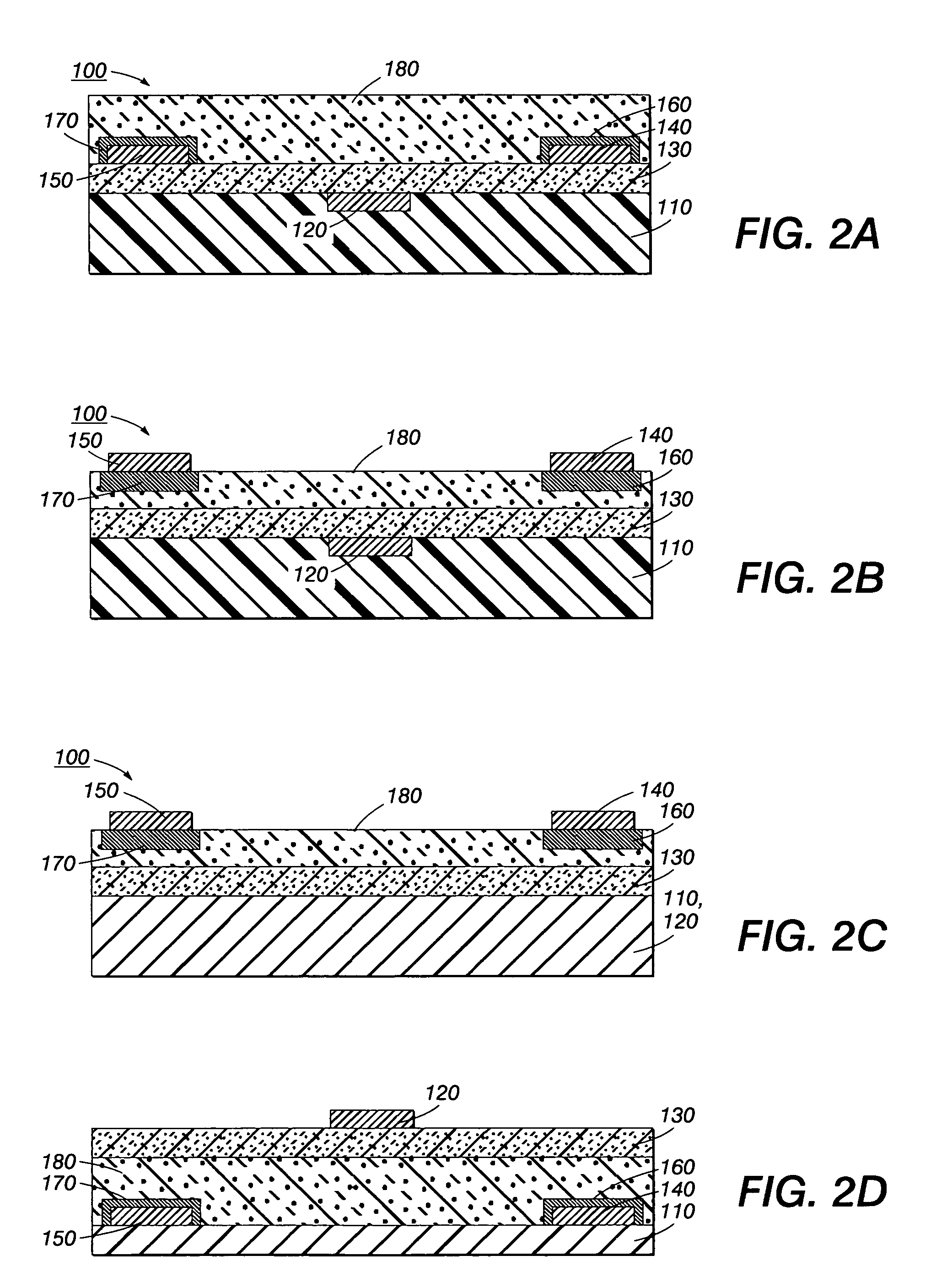
[0005]In embodiments, the present disclosure is directed to the reduction of contact resistance between the electrodes and the semiconductor layer by increasing the conductivity of the semiconductor at the region which is close to the electrode (or “contact region”). This can be accomplished by doping the contact regions with appropriate dopants or dopant precursors ad discussed in more detail below.
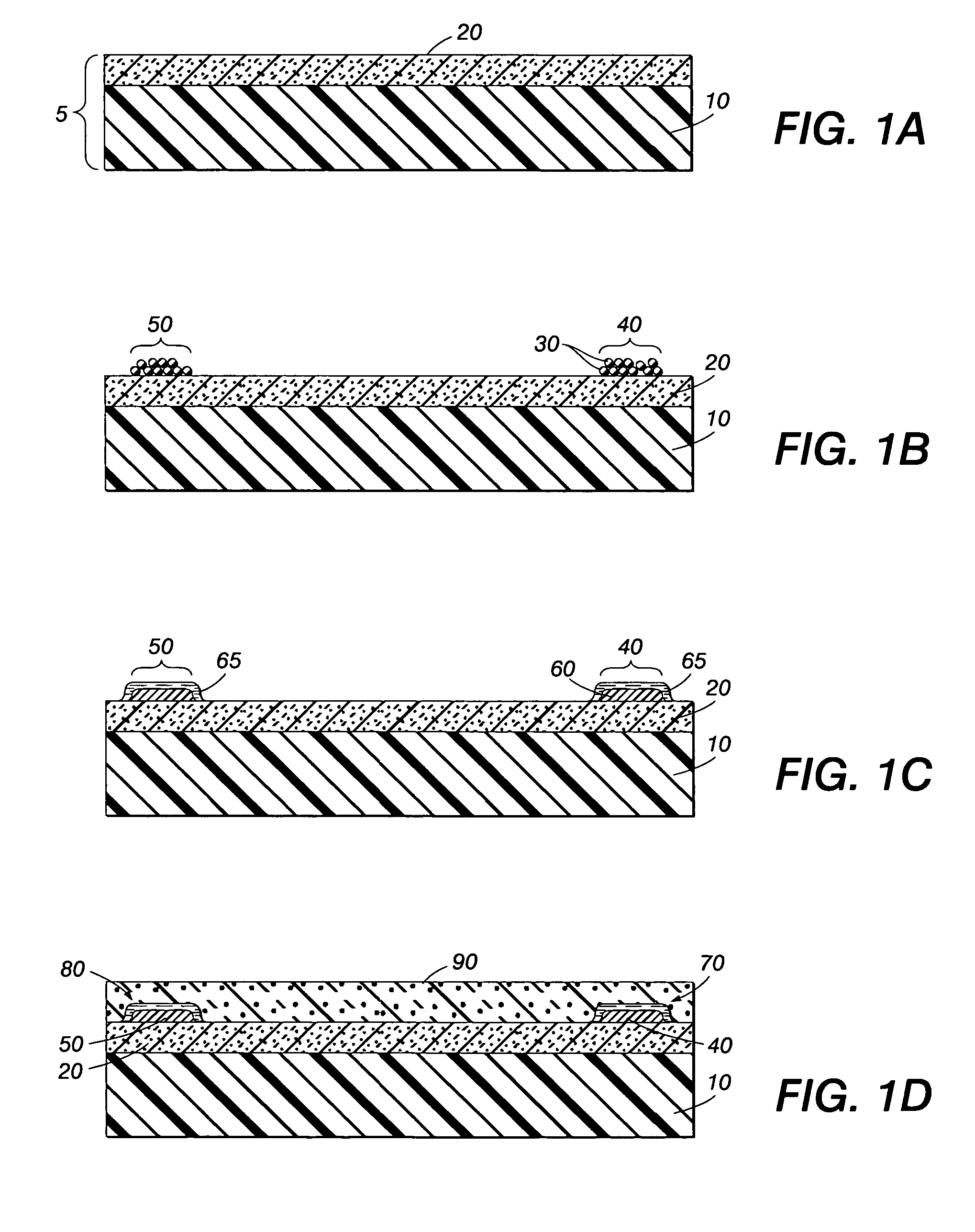
[0007]In another embodiment, a substrate is provided. Dopant or dopant precursor-stabilized metal nanoparticles such as acid-stabilized metal nanoparticles are used to deliver a dopant or chemically reacted dopant (which is a product of the dopant precursor after reaction or decomposition) to a contact region of the semiconductor layer. Upon annealing, the metal nanoparticles coalesce and form an electrically conductive electrode and the dopant or chemically reacted dopant is released. Upon deposition of a semiconductor layer, the dopant or chemically reacted dopant diffuses into the semiconductor layer and forms a contact region. This method delivers dopant or chemically reacted dopant to the region where it has its greatest efficacy and deposits the electrode and the dopant in one single step, whereas in conventional processes the electrode and dopant were separately deposited. This embodiment therefore simplifies the manufacture of an OTFT and reduces costs.

Problems solved by technology

TFT circuits using current mainstream silicon technology may be too costly for some applications, particularly for large-area electronic devices such as backplane switching circuits for displays (e.g., active matrix liquid crystal monitors or televisions) where high switching speeds are not essential.
The high costs of silicon-based TFT circuits are primarily due to the use of capital-intensive silicon manufacturing facilities as well as complex high-temperature, high-vacuum photolithographic fabrication processes under strictly controlled environments.
However, little attention has been given to the optimization of interfacial properties between the source / drain electrodes and the semiconductor layer, which often give rises to contact resistance.

Method used


Image

  • Methods to minimize contact resistance
  • Methods to minimize contact resistance
  • Methods to minimize contact resistance

Examples


example 1

[0040]An n-doped silicon wafer with a 100-nm silicon oxide layer was used as substrate. The doped wafer functioned as the gate electrode and the silicon oxide layer functioned as the gate dielectric which had a capacitance of about 30 nanofarads per square centimeter (nF / cm2) as measured with a capacitor meter. The silicon oxide surface was first cleaned with argon plasma and then immersed in a 0.1 M solution of octyltrichlorosilane (OTS-8) in toluene at 60° C. for 20 minutes to form a self-assembly monolayer. A solution of oleic acid-stabilized silver nanoparticles (prepared according to Lin, X. Z, et al., Langmuir, 2003, 19, 10081.) in cyclohexane (5-wt %) was spin-coated on the OTS-8-modified silicon wafer. After annealing at 200° C. for 45 min, a highly conductive thin film was formed. The conductivity of the thin film was measured to be 2×10⁴ S / cm. The conductive thin film was mechanically patterned into electrodes with channel length of 19 μm and channel width of 1600 μm. The ...


PUM

PropertyMeasurementUnit
temperatureaaaaaaaaaa
thicknessaaaaaaaaaa
thicknessaaaaaaaaaa

Abstract

A method is disclosed for making a metal electrode which minimizes the contact resistance between it and an organic semiconductor. Acid-stabilized metal nanoparticles are deposited upon a substrate and annealed. This creates a metal electrode and releases acid. Upon deposition of semiconductor and subsequent annealing, the acid diffuses from the electrode into the semiconductor layer and acts as a dopant, minimizing the contact resistance. The use of oleic acid-stabilized silver nanoparticles is demonstrated.

Description

[0001]The U.S. Government has a paid-up license in this development and the right in limited circumstances to require the patent owner to license others on reasonable terms as provided for by the terms of NIST Contract No. 70NANBOH3033.BACKGROUND[0002]The present disclosure relates to methods for making electrically conductive electrodes for electronic devices, such as organic thin-film transistors (“OTFT”s), with no or minimum contact resistance between the electrodes and the semiconductor. The present disclosure also relates to electronic devices produced by such methods.[0003]Thin film transistors (TFTS) are fundamental components in modern-age electronics, including, for example, sensors, image scanners, and electronic display devices. TFT circuits using current mainstream silicon technology may be too costly for some applications, particularly for large-area electronic devices such as backplane switching circuits for displays (e.g., active matrix liquid crystal monitors or tele...

Claims


Application Information

Patent Timeline
Patent Type & Authority Patents(United States)
IPC IPC(8): H01L51/40
CPCB82Y20/00B82Y30/00H01L51/0545H01L51/105H01L51/0541H01L2251/5369H10K10/464H10K10/466H10K10/84H10K2102/331
Inventor WU, YILIANGONG, BENG S.LI, YUNING
Owner XEROX CORP
Why Eureka
Try Eureka