Arrays of microparticles and methods of preparation thereof

Active Publication Date: 2008-02-26
BIOARRAY SOLUTIONS
View PDF51 Cites 45 Cited by
  • Summary
  • Abstract
  • Description
  • Claims
  • Application Information

AI Technical Summary

Benefits of technology

[0028]The present invention provides a parallel processing method that takes advantage of semiconductor fabrication methods. In addition, the methods in this invention are flexible enough to address different quantity and different assay requirements. The invention combines the flexibility of being able to select the array content with the high feature density and economies of scale afforded by parallel (batch) array assembly. This invention provides a process for the assembly of random encoded, solid carrier-displayed probe arrays of selectable composition in designated positions within delineated compartments on a substrate which may then be fractionated into a plurality of chips having arrays of carrier-displayed probes. In

Problems solved by technology

The deposition, printing and spotting methods for probe array production have several undesirable characteristics.
First, even state-of-the-art deposition and printing technologies only produce arrays of low feature density, reflecting typical spot dimensions of 100 microns and spot-to-spot separations of 300 microns.
Second, methods of probe deposition described to date have failed to produce uniform spots, with significant spot-to-spot variations.
Third, spotting methods, including such variants as electrophoretic deposition to patterned electrodes [U.S. Pat. No. 5,605,662], require substantial instrumental and logistical support to implement the production of arrays on any significant scale.
In particular, spotting methods do not support batch fabrication of probe arrays.
That is, while a batch processing format may be used to produce substrates efficiently, the subsequent step of “bio-functi

Method used


Image

  • Arrays of microparticles and methods of preparation thereof
  • Arrays of microparticles and methods of preparation thereof
  • Arrays of microparticles and methods of preparation thereof

Examples


Example

Example 1

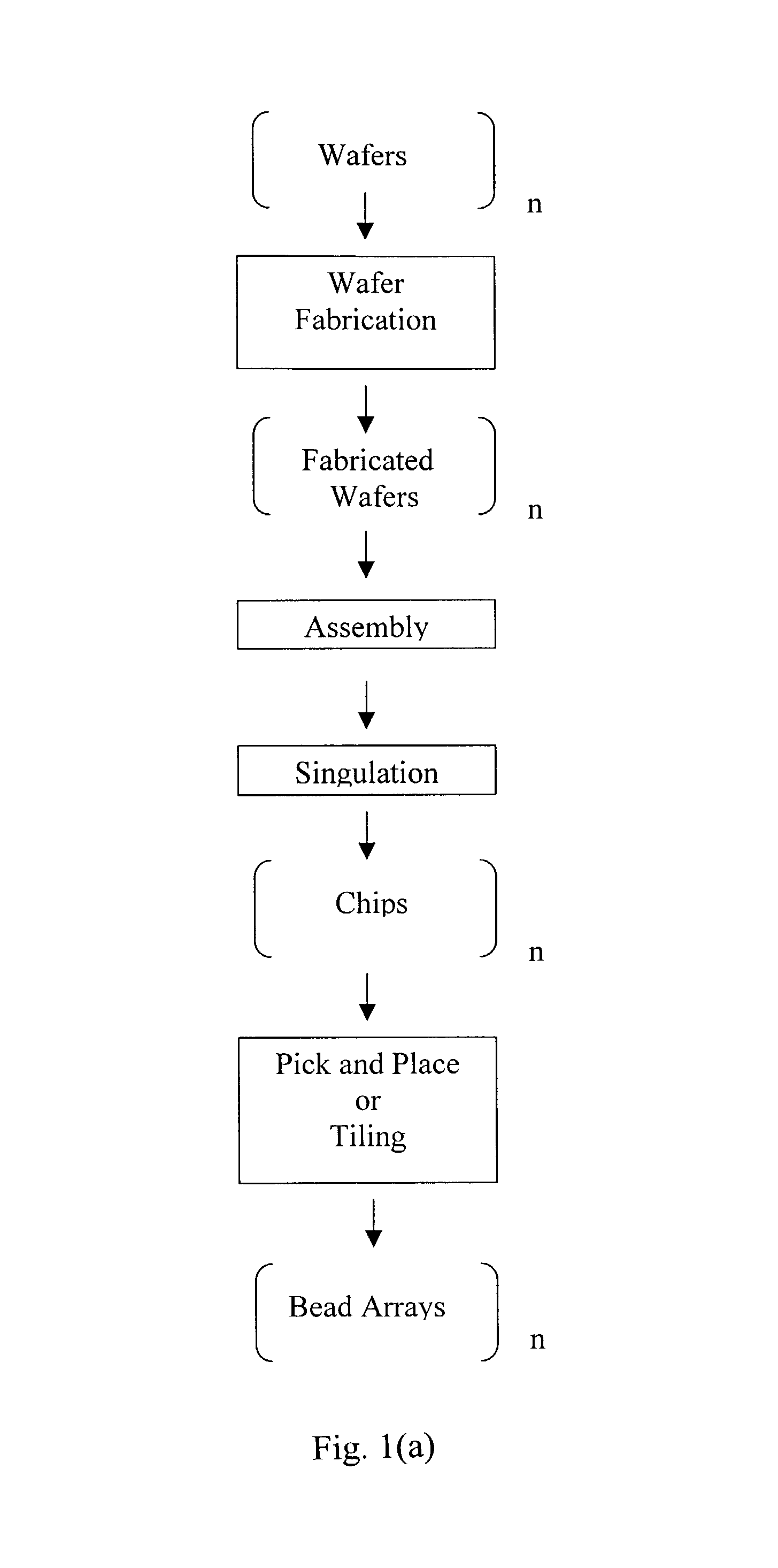
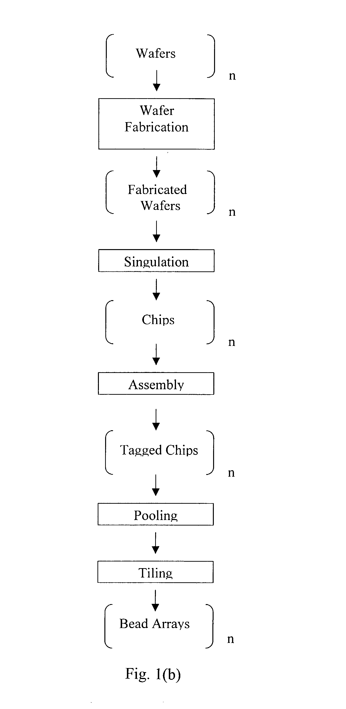
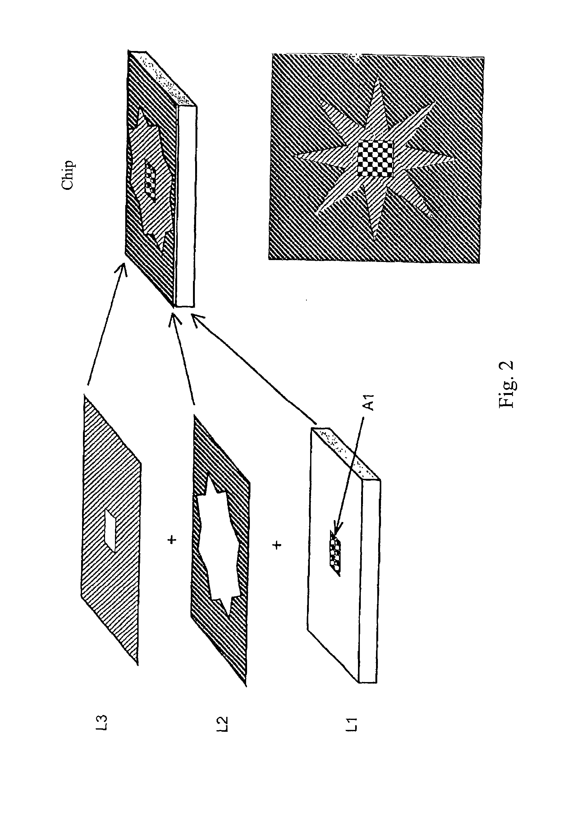
Wafer Fabrication and Design of Chips Comprising Bead Arrays

[0111]The fabrication process of the chip comprising a bead array, as shown in FIG. 4, is described in FIG. 11. The substrate was a 100 mm diameter, 0.5 mm thick, silicon wafer with crystal orientation of (100), n-type phosphorus doped. A suitable resistivity range for these wafers is 1.5-4Ω-cm. Wafers were usually fabricated in batches of up to 25. The first step comprises SiO2 growth. The wafers were first cleaned by the RCA cleaning process, which comprises the steps of (1) soaking the wafers in a mixture of NH4OH:H2O2 (30%):H2O in a volume ratio of 1:1:5 at 75° C. for 10 minutes; (2) rinsing with a cascade water batch cleaning using 18 MΩ-cm water; (3) soaking the wafers in a mixture of HCl (36%):H2O2 (30%):H2O in a volume ratio of 1:1:5 at 75° C. for 10 minutes; and (4) rinsing with a cascade flow water batch cleaning until the water in the bath is at least 16 MΩ-cm. The wafers were spun dry before being place...

Example

Example 2

Functionalization of Beads and Formation of a Bead Array

[0117]Color encoded, tosyl-functionalized beads of 3.2 μm diameter were used as solid phase carriers. Several sets of distinguishable color codes were generated by staining particles using standard methods (Bangs. L. B., “Uniform Latex Particles”, Seragen Diagnostics Inc., p.40). Stained beads were functionalized with Neutravidin (Pierce, Rockford, Ill.), a biotin binding protein, to mediate immobilization of biotinylated probes or primers. In a typical small-scale coupling reaction, 200 μl of suspension containing 1% beads were washed three times with 500 μl of 100 mM phosphate buffer / pH 7.4 (buffer A) and resuspended in 500 μl of that buffer. After applying 20 μl of 5 mg / ml neutravidin to the bead suspension, the reaction was allowed to proceed overnight at 37° C. Coupled beads (i.e., beads with bio-functional molecules attached thereto) were then washed once with 500 μl of PBS / pH 7.4 with 10 mg / ml BSA (buffer B), re...

Example

Example 3

Forming a Bead Array

[0122]A bead slurry was directly dispensed onto the array area on a chip. A wet cotton applicator (K1) was used to gently stir the bead slurry on the array surface. The motion of K1 can be circular, linear or some other meaningful mode, and is usually parallel to the chip surface. After stirring the slurry several times, the beads were moved into the array. Then, the chip surface was cleaned by using K1 to wipe away extra beads that were not in the array. This process can be scaled up from single chips to wafer-scale multi-chip assembly, and can be automated.

[0123]An example of a processing procedure for forming bead arrays is as follows. Two microliters of 1% microparticles (approximately 3.2 micrometers in diameter) in 100 microliters of phosphate-buffered saline (also known as PBS: 150 mM, NaCl; 100 mM, NaP, pH 7.2) were used for assembling eight microparticle arrays on silicon chips (2.5×2.5 mm) with 4,000 microwells on each chip. The following proce...


PUM

PropertyMeasurementUnit
Frequencyaaaaaaaaaa
Frequencyaaaaaaaaaa
Frequencyaaaaaaaaaa

Abstract

This invention provides high unit density arrays of microparticles and methods of assembling such arrays. The microparticles in the arrays may be functionalized with chemical or biological entities specific to a given target analyte. The high unit density arrays of this invention are formed on chips which may be combined to form multichip arrays according to the methods described herein. The chips and/or multichip arrays of this invention are useful for chemical and biological assays.

Description

[0001]This application claims priority to U.S. Provisional Application 60 / 343,621 filed on Dec. 28, 2001. U.S. Provisional Application 60 / 343,621 is hereby incorporated by reference in its entirety.FIELD OF THE INVENTION[0002]This invention relates to high unit density arrays of microparticles and methods of making same. This invention also relates to multichip arrays and their methods of manufacture. This invention further provides methods for performing bioassays using high unit density arrays and multichip arrays.BACKGROUND OF THE INVENTION[0003]An array format for biological and chemical analysis holds the promise to rapidly provide accurate results while minimizing labor. [Nature Genetics, 1999 Vol. 21 (1) supplement pp.3-4] Typically, arrays of biological probes such as DNA, RNA or protein molecules are formed either by deposition and immobilization or by in-situ synthesis on inert substrates. In these prior art methods, array formation is usually accomplished by attaching pro...

Claims


Application Information

Patent Timeline
IPC IPC(8): C40B20/02B01J19/00C07H1/00G01N37/00C07H21/00C12M1/34C12NG01NG01N33/53G01N33/533G01N33/543H01L21/00
CPCB01J19/0046C12Q1/6837B01J2219/00274B01J2219/00317B01J2219/00466B01J2219/00468B01J2219/005B01J2219/00545B01J2219/00648B01J2219/00662C12Q2563/149G01N33/5302G01N33/54306
Inventor SEUL, MICHAELCHAU, CHIU WOHUANG, HUIBANERJEE, SUKANTAYANG, JIACHENGHONG, YE
Owner BIOARRAY SOLUTIONS
Why Eureka
Try Eureka